|

|
Forum Index : Electronics : Various aspects of home brew inverters
| Author | Message | ||||
| Solar Mike Guru Joined: 08/02/2015 Location: New ZealandPosts: 1203 |
Hey TinyT, pin 11 on these chips floats between 0 and 48v and is a virtual earth for upper mosfet gate drive, there shouldn't be any resistor there R8//14. Cheers Mike |
||||
| tinyt Guru Joined: 12/11/2017 Location: United StatesPosts: 556 |
Have to trace back thru this thread where I did it. I think it is because of this. Perhaps pin 11 should have a pull down in case of input disconnect, will fail safe. (or is there an internal pull down ?) Rest looks good. I still dont get what is happening with the buss wires on the PDF's I have tried 4 different PDF viewers and none show me the bussed wires - I now give up - I dont need to see them, just not sure why I cant. You are right. Here is revised schematic for review/comments. 2018-11-22_143912_NANOVERTERdraft9.pdf I have removed the resistors. Since the ST_SP_SIG is momentary like a non latching push button, I have also added an LED for visual indication that the PWM is on. I hope poida will support it in his code. |
||||
| wiseguy Guru Joined: 21/06/2018 Location: AustraliaPosts: 1267 |
I see the problem - lets add some red and rearrange slightly I assume all the unused pins on the nano have internal pullup/downs as required ? Perhaps pin 11 (referring to the input on off switch on the nano)should have a pull down in case of input disconnect, will fail safe. (or is there an internal pull down ?) Rest looks good. Sorry for the ambiguous post - why did they both have to be pin 11...... If at first you dont succeed, I suggest you avoid sky diving.... Cheers Mike |
||||
| tinyt Guru Joined: 12/11/2017 Location: United StatesPosts: 556 |
I assume all the unused pins on the nano have internal pullup/downs as required ? Perhaps pin 11 (referring to the input on off switch on the nano)should have a pull down in case of input disconnect, will fail safe. (or is there an internal pull down ?) Rest looks good. Sorry for the ambiguous post - why did they both have to be pin 11...... Apologies also. English is my second language.  |
||||
| nickskethisniks Guru Joined: 17/10/2017 Location: BelgiumPosts: 472 |
Hi, isn't it necessary to add ceramic capacitors on the in/outputs of the lineair voltage regulators to prevent osccilatons? |
||||
| Tinker Guru Joined: 07/11/2007 Location: AustraliaPosts: 1904 |
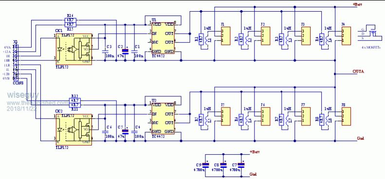
 2018-11-22_005206_Output_PCB_Sch.pdf Schematic picture is a bit ordinary so PDF uploaded here Wiseguy, I'm looking at your schematic with interest and have a few questions if you don't mind. What does the 1uH inductor at the gate do? I have not seen that idea before. Why the 4R7 series resistors in the 12V supply for the opto & gate driver chip? And two comments: You should feed the +Bat directly to the drains via the heatsink, not via the connectors as shown. Ditto for the source/drain connection (OUT A/B). But you knew that anyway  . .3 x 4700uF capacitors per 8 mosfet half bridge board is not a lot, I would have used 2 x 10,000uF. I'm also curious which isolated 12V supplies you chose. Warpspeed suggested to use AC to DC supplies and I bought some. Much to my surprise I could get the full rated 2Amps @12V when powering them from 50V DC. Klaus |
||||
| poida Guru Joined: 02/02/2017 Location: AustraliaPosts: 1464 |
If nano1 code and IO assignment is complete, can we now continue to nano2 pin assignments? I was just thinking that now too. I think nano1 code is pretty much ready for serious testing. I want to stress again that this project is NOT for connecting to street power under any circumstances. Doing so will likely cause much trouble in your life and involve visits from very pissed off electrical supply company people. That being said, let's see what it can do and if it blows inverter boards up. I want to start on nano2 now. My feature list: - use 20 x 4 line or 16 x 2 line LCD if present, via i2c or SPI. - use the USB serial port for set up and sensor/inputs calibration - use the USB serial port for programming of the nanos - provide a very simple API via the USB serial port to enable: 1 - start and stop of inverter 2 - query operating parameters, eg. AC volts out, DC volts in, DC current in - the already detailed DC LV cut off and DC V restart when appropriate, DC over current cutoff, etc I think this is where we will get a bit more input from the forum and I welcome that. Nano1 code is something I am quite happy with and I have a high expectation that it will perform well. When synchronising to an AC master, we might discover problems. This is new territory for me. The code is simple and robust and that is what we need. wronger than a phone book full of wrong phone numbers |
||||
| brac321 Regular Member Joined: 30/11/2016 Location: SloveniaPosts: 54 |
Yes, it is. Without they can produce unpredictable impulses and oscillations! 100nF as close as possible to their inputs and outputs is mandatory. Like here on one of my old projects. OffGrid 24/7: 250w black mono solar panels 6.4kWp, 1x Midnite Classic 150, 1x MorningStar MPPT 60, battery bank 840 Ah @ 48v, modified LF-8K inverter, DC/DC, hot water harvesting, etc. |
||||
| tinyt Guru Joined: 12/11/2017 Location: United StatesPosts: 556 |
Here is revised schematic for review/comments. 2018-11-22_235219_NANOVERTERdraft10.pdf It is now in two pages. I have added 104 caps at the linear regulator input and output pins. I have added 10K pull-ups to help the weaker internal pull up at nano D8. The Atmega328 spec says it can range from 20K to 50K. The paralleled 10K should make it more immune to noise, I think. Nano2 has support for two fans and two temperature sensing. I took the liberty of assigning all the analog inputs, except those used by I2C. I hope it is OK. |
||||
| wiseguy Guru Joined: 21/06/2018 Location: AustraliaPosts: 1267 |
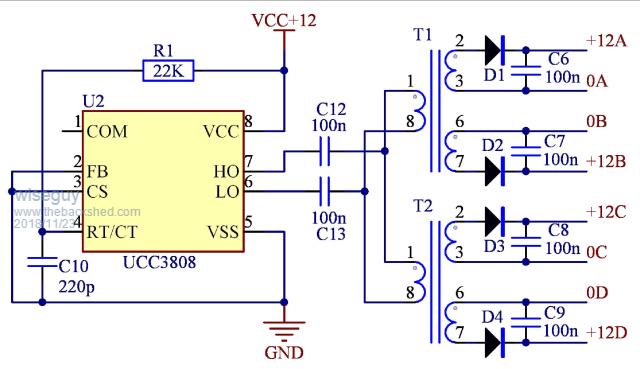
Wiseguy, I'm looking at your schematic with interest and have a few questions if you don't mind. What does the 1uH inductor at the gate do? I have not seen that idea before. When paralleling multiple FETs from a common drive there can be a tendency for them to oscillate spuriously. The cure is to add HF impedance in the circuit, this can take the form of ferrite beads on the legs of the FETs or seperate gate resistors or and with separate inductors also for each gate. Google "APT-0402" Application note for an excellent explanation of the issue. Another App note about parallel mosfets Here Why the 4R7 series resistors in the 12V supply for the opto & gate driver chip? I like having some impedance between high current noisy parts of the circuit and the control board environment. The resistors can be replaced with axial inductors if noise is an issue. Also for the Lower FETs of the two half bridge PCBs any imbalance of currents will not force high currents through the low energy connector and wiring. In theory, a difference of 0.1V and 1 milliohm of resistance can cause 100A to try to flow. Now repeat with 4.7 ohms and it becomes 0.1/4.7001 or 21 milliamps. The resistors have essentially no effect to the current levels required by the drive circuits powered from the isolated 12V supplies. And two comments: You should feed the +Bat directly to the drains via the heatsink, not via the connectors as shown. Ditto for the source/drain connection (OUT A/B). But you knew that anyway  . .Yes Im afraid I did  My plan was to use multiple individual equal length wires. My plan was to use multiple individual equal length wires.When the FETs are inserted into the J connectors (Warp style) a wire is also inserted with the Drain and Source. Now join the 4 wires together and they become the Batt+, Batt- and Bridge to Toroidal Nodes. Remember this is a prototype to prove the concept & function, so this type of "hacking" is cheap and forgivable. My FET boards will be 50mm x 100mm and the control board is planned for 100mm x 100mm - because that is the most economical size from PCBWAY - 10 boards for ~$20au. so I will get back 20 Fet boards and 10 control boards for ~$40. 3 x 4700uF capacitors per 8 mosfet half bridge board is not a lot, I would have used 2 x 10,000uF. How much room do you reckon is left on a 50mm x 100mm FET board with 8 connectors for FETs, optocouplers, driver ICs, input connector etc - 3 x 4700uF is all that will now fit !  I'm also curious which isolated 12V supplies you chose. Warpspeed suggested to use AC to DC supplies and I bought some. Much to my surprise I could get the full rated 2Amps @12V when powering them from 50V DC. I rolled my own it is an RM6 core using a power bobbin (8 pins). Primary 18T of 0.2mm 3 x secondaries each 20T of 0.2mm done ! Add5 parts for a couple of dollars finished ! Its 2.00am Im too tired to redraw this properly - only T1 is used and pins 4 & 5 will have the third winding, it is a fairly simple & efficient circuit.  If at first you dont succeed, I suggest you avoid sky diving.... Cheers Mike |
||||
| brac321 Regular Member Joined: 30/11/2016 Location: SloveniaPosts: 54 |
Tiny, may I suggest something about board routing. When drawing a PCB (or autorouting) to avoid entering most of RF disturbances trough the air from outside world in to circuit itself, and also transmitting out any internal RF noise, it is important to have a wide Faraday cage (connected to GND or "-" level) all around PCB on each layer, if there is multilayer PCB to be designed. Something like here on my boards: sample 1 , sample 2 , sample 3 ... English is my second language OffGrid 24/7: 250w black mono solar panels 6.4kWp, 1x Midnite Classic 150, 1x MorningStar MPPT 60, battery bank 840 Ah @ 48v, modified LF-8K inverter, DC/DC, hot water harvesting, etc. |
||||
| tinyt Guru Joined: 12/11/2017 Location: United StatesPosts: 556 |
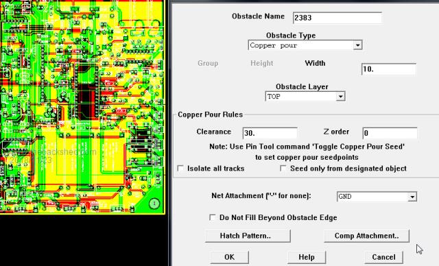
Something like here on my boards: sample 1 , sample 2 , sample 3 ... English is my second language Yes, that is what I will do. In orcad layout, they call it copper pour, like this:  . .To keep the cost down, the board will have only two layers. This is good, people from other countries are contributing. I am not an expert in pcb designing, so I will need all the help to make this successful. |
||||
| brac321 Regular Member Joined: 30/11/2016 Location: SloveniaPosts: 54 |
My boards are all manually routed, I do not trust autoruters. Sometimes is the length of tracks and their capacity important, sometimes their position and layout. Autorouters don't do that properly at all. Tracks need to be wide enough for expected currents, vias too. And in case of Nanoverter there won't be any special designing rules required like for PCB's that operate on a RF (high frequencies). If I guess, you are already familiar with all those basics needed to design Nanoverter PCB's. OffGrid 24/7: 250w black mono solar panels 6.4kWp, 1x Midnite Classic 150, 1x MorningStar MPPT 60, battery bank 840 Ah @ 48v, modified LF-8K inverter, DC/DC, hot water harvesting, etc. |
||||
| poida Guru Joined: 02/02/2017 Location: AustraliaPosts: 1464 |
Tinyt: initial code for nano2 requires D7 output to lead to nano1 D8, used for inverter on/off All analog inputs remain the same. #define ADC_OUT 0 // channel for AC output sample #define ADC_DCI 3 // DC current sense #define ADC_HS 2 // Heat sink temp sensor #define ADC_DCV 1 // DC supply volts sample I am coding to use a 20x4 LCD, connected through I2C. I like I2C, it uses only 4 wires, 5V, ground, sda, scl. I want to code only for 20x4 sized LCD, 20 characters by 4 lines. Ebay has them for about $10 delivered Jaycar too, but it will cost you about $35 Any objections to my choice of display? The code will permit requesting all the display data via the serial connection anyway, this will be handy for me at least. But it offers flexible option for other designs. wronger than a phone book full of wrong phone numbers |
||||
| tinyt Guru Joined: 12/11/2017 Location: United StatesPosts: 556 |
Tracks need to be wide enough for expected currents, vias too. And in case of Nanoverter there won't be any special designing rules required like for PCB's that operate on a RF (high frequencies). If I guess, you are already familiar with all those basics needed to design Nanoverter PCB's. I am glad the nanoverter does not operate in RF, I don't have the skills to do RF. I cannot even do manual routing. I hope autorouting is good enough for the nanoverter, otherwise I might need your help. |
||||
| noneyabussiness Guru Joined: 31/07/2017 Location: AustraliaPosts: 527 |
Just a suggestion, to simplify mosfet driving requirements... hip4082 ... cheap and complete with only 1 chip driving mosfets.. I think it works !! |
||||
| tinyt Guru Joined: 12/11/2017 Location: United StatesPosts: 556 |
initial code for nano2 requires D7 output to lead to nano1 D8, used for inverter on/off All analog inputs remain the same. #define ADC_OUT 0 // channel for AC output sample #define ADC_DCI 3 // DC current sense #define ADC_HS 2 // Heat sink temp sensor #define ADC_DCV 1 // DC supply volts sample I am coding to use a 20x4 LCD, connected through I2C. I like I2C, it uses only 4 wires, 5V, ground, sda, scl. I want to code only for 20x4 sized LCD, 20 characters by 4 lines. Ebay has them for about $10 delivered Jaycar too, but it will cost you about $35 Any objections to my choice of display? The code will permit requesting all the display data via the serial connection anyway, this will be handy for me at least. But it offers flexible option for other designs. Here is revised schematic for review/comments. 2018-11-23_113027_NANOVERTERdraft11.pdf I have transferred the net at D5 to D7. I have switched ADC2 and ADC3 usage to match with code. Not sure if ADC6 and ADC7 will be used but I have made connections to them. I have also added direct connections to the RX and TX of the nano in case others will not use the Arduino IDE for serial communication. |
||||
| Solar Mike Guru Joined: 08/02/2015 Location: New ZealandPosts: 1203 |
TinyT: >> Here is revised schematic for review/comments. 2018-11-23_113027_NANOVERTERdraft11.pdf Just a suggestion, those transistors you have for the fan control could be upgraded to a small mosfet; some fans draw up to 400 ma, the PN2222 is really only good for 100ma or so, I use DMN6075S-7 N-Channel MOSFET, 2.5 A, 60 V, 3-Pin SOT-23 logic level devices for things like fans\relays etc, RS #921-1280, just make sure the gate has a 10k pull-down. noneyabussiness: Hip4082, great suggestion and would simplify drive requirements; however for those wanting to use the nanoInverter to drive an existing OzInverter H-Bridge that doesnt have extra totem pole or other boosted drivers, will be out of luck, the Hip4082 doesnt have enough drive current for multiple parallel mosfets. For those of us using opto drivers it would be ideal, the whole chip could be run off 12v and drive the opto's directly. Cheers Mike |
||||
| tinyt Guru Joined: 12/11/2017 Location: United StatesPosts: 556 |
TinyT: >> Here is revised schematic for review/comments. 2018-11-23_113027_NANOVERTERdraft11.pdf Just a suggestion, those transistors you have for the fan control could be upgraded to a small mosfet; some fans draw up to 400 ma, the PN2222 is really only good for 100ma or so, I use DMN6075S-7 N-Channel MOSFET, 2.5 A, 60 V, 3-Pin SOT-23 logic level devices for things like fans\relays etc, RS #921-1280, just make sure the gate has a 10k pull-down. .......Cheers Mike I think we are trying to avoid small surface mount chips. Here is a screen capture of a digikey(US distributor) search for TO92 mosfet, but I don't know if they are readily available in other countries. Edit: jpg is unreadable, changed to print out of spreadsheet. 2018-11-23_132856_MosfetDigikey.pdf If SOT223 can be soldered by most of us, let me know the part number of what is readily available. Or we can use the bigger TO-220 package. Maybe configure the PN2222 as darlingtons will be good enough. I think they will still be cheaper. |
||||
| Solar Mike Guru Joined: 08/02/2015 Location: New ZealandPosts: 1203 |
Maybe configure the PN2222 as darlingtons will be good enough. I think they will still be cheaper. Sot223 is easily solderable many logic types available: NTF3055L: AliExpress FDT3612 AliExpress The small 92 type packages are harder to locate with any current carrying capacity. Cheers Mike |
||||
| The Back Shed's forum code is written, and hosted, in Australia. | © JAQ Software 2026 |