
|

|
Forum Index : Electronics : Various aspects of home brew inverters
| Author | Message | ||||
Madness Guru Joined: 08/10/2011 Location: AustraliaPosts: 2498 |
Gidday John, Only 2 types, the baby 4KW version and the 8KW. The 8KW as you have has 104 caps on the low side and 5K1 between the source and gate drive on high and low side before it goes through the 10R gate resistors. This image is from a later version that I have not had made yet, the main difference is screw terminals for the negative input. The components are the same and in the same positions, I still have a number of the current version so won't be getting this new version for a while yet. 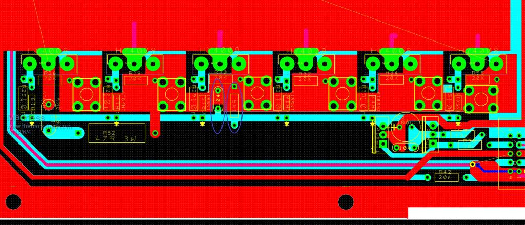 There are only 10 types of people in the world: those who understand binary, and those who don't. |
||||
| johnmc Senior Member Joined: 21/01/2011 Location: AustraliaPosts: 282 |
Thanks Madness Found the 104 cap and 5K1 resistor  johnmc |
||||
| Tinker Guru Joined: 07/11/2007 Location: AustraliaPosts: 1904 |
Hi Gary, how do you get that .gif image from your PCB layout program? I have tried to get a colour version of my PCB's printed from Design Spark but so far managed only B&W pictures which are useless. Thanks. Klaus |
||||
| wiseguy Guru Joined: 21/06/2018 Location: AustraliaPosts: 1267 |
Hi Andrew in my post I believe I/(we) said exactly the same thing. English is my first language but sometimes I wonder.... "I have seen that FETs can have a tendency to oscillate if they travel too slowly through the miller region" I believe that negative gate drive glitch at the plateau end kick-started the oscillation. "Then there is the Cgd (~75nC) that injects opposite polarity charge to the gate drive and slows down the drive further, the higher the drain voltage being switched the greater the (bad) effect Cgd has on the drive signal. I believe it is this effect that is visible in the last picture trying to turn off the gate drive as the drain voltage rapidly falls as the FET turns on" In the past when I have encountered this issue, more drive current (lower impedance drive) usually helps overcome this crappy effect of Cgd. The faster you switch FETs the worse the effect of Cgd. I'm also happy to be wrong but even happier if right. If at first you dont succeed, I suggest you avoid sky diving.... Cheers Mike |
||||
| hugocamaras Newbie Joined: 12/04/2019 Location: BrazilPosts: 24 |
Madness, their power boards with totems, I can only have access to them buying them ready with you or can you make pdf files available with the top, bottom and silk copper strips in pdf? |
||||
Madness Guru Joined: 08/10/2011 Location: AustraliaPosts: 2498 |
@hugocamaras Sorry I put a lot of work into the design and for a number of reasons I am not releasing anything other than the boards themselves. Aurth8 is supposed to be organising getting some to Brazil very quickly, it would pay to get in touch with him. There are only 10 types of people in the world: those who understand binary, and those who don't. |
||||
Madness Guru Joined: 08/10/2011 Location: AustraliaPosts: 2498 |
 Hi Gary, how do you get that .gif image from your PCB layout program? I have tried to get a colour version of my PCB's printed from Design Spark but so far managed only B&W pictures which are useless. Thanks. The photo above was a screenshot that I cropped. You can print in colour by unticking the print setting that says print all colours Black. 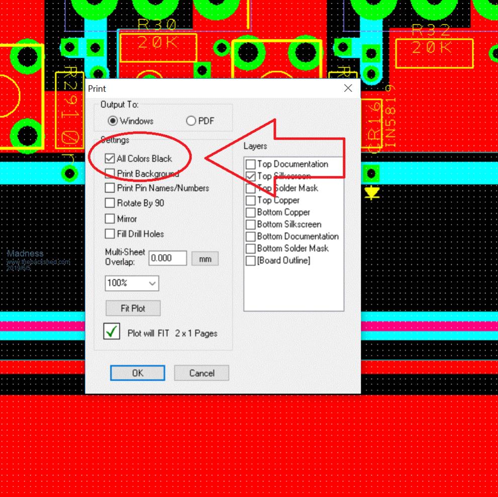 There are only 10 types of people in the world: those who understand binary, and those who don't. |
||||
mackoffgrid Guru Joined: 13/03/2017 Location: AustraliaPosts: 460 |
Mike. Nicely summed up  |
||||
| Tinker Guru Joined: 07/11/2007 Location: AustraliaPosts: 1904 |
Thanks Gary, found that page, changed it to your settings and it worked a treat  Klaus |
||||
| poida Guru Joined: 02/02/2017 Location: AustraliaPosts: 1464 |
I just had a look at the high side gate voltage and current, in the middle of the 1/2 cycle, maybe about 5ms in from zero crossing. I have approx. 0.4uH ferrite beads on the gate pins of both low and high side MOSFETS. Other than that it is the normal test conditions (27.5V DC supply, 50uH choke, small toroid, "10" uF cap which is actually 6uF) The power board is Madness' board, with one HY4008 fitted at each leg of the full bridge. 10R gate resistors, totem pole drive, 5KR gate to Source pulldown resistors. First, the DSO saw this: Light Blue is Gate Voltage, DC coupled and referenced to DC ground. Dark Blue is Gate resistor current (the voltage across the 10R resistor) 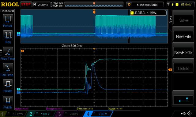 And we see non-optimal switching, with some oscillation. I obtained the values of this DSO capture and after a bit of Excel goodness we have: Black is Gate Voltage, Light Green is current and Grey is accumulated Charge The left hand scale is correct for current, the peak is nearly 0.8A, and it's scaled for charge, 0.4 = 400nC The time scale is in seconds, each marker = 1 uS. The switch event starts at 2.5uS and is all over at about 3.2uS. 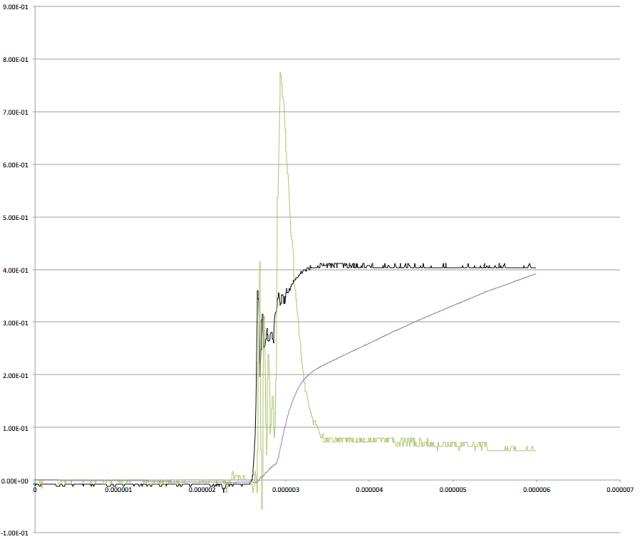 So it seems the HY4008 total Gate charge (190nC from the specs.) is achieved well after the oscillations. 2019-06-05_205516_NewFile1.xls.zip Here is the low side switch event at about the same time in the 1/2 wave (5mS) Note the lower current. 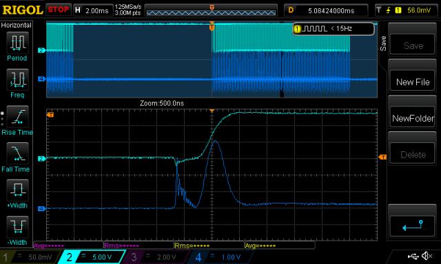 and 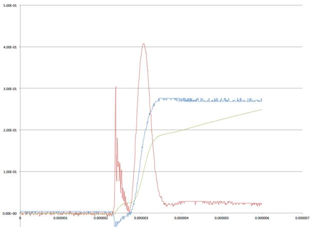 (different colours but we can deal with that..) 2019-06-05_211857_NewFile2.xls.zip It looks rather different, don't you think? The gate voltage clearly starts at some negative value (good, I like that for shoot through control) and powers up about as fast as the high side. Fuel for discussion. And this is by no means a critique of Madness' power board. I think it's a great board and I am likely to power my home by it in the near future. The ferrite beads are not part of the specified build and are simply present at this moment in time. I am exploring the effect of things I can do to the board. wronger than a phone book full of wrong phone numbers |
||||
Madness Guru Joined: 08/10/2011 Location: AustraliaPosts: 2498 |
Fitting beads to those MOSFETs is rather difficult unless you leave at least 5mm extra gap between the board and the MOSFET. Ferrite beads are used on the Powerjack boards with TO220 MOSFETs and very long legs. There are only 10 types of people in the world: those who understand binary, and those who don't. |
||||
| wiseguy Guru Joined: 21/06/2018 Location: AustraliaPosts: 1267 |
Good work Poida, want to make sure I understand this setup. Are the 0.4uH ferrite beads discussed here used in a normally configured Madness board or is this something recently added to the gates for evaluation ? If recently added, are there wave-forms minus beads which hopefully you could probably point me to them from a previous post somewhere ? Can you also confirm that there are no beads for these scope shots on the Drains ? The red spike at the beginning of the second graph is a surprise - havent figured out what is causing that yet. I assume it coincides with the turn off of the upper side FET ? If at first you dont succeed, I suggest you avoid sky diving.... Cheers Mike |
||||
| poida Guru Joined: 02/02/2017 Location: AustraliaPosts: 1464 |
Mike, the test used the ferrite beads, placed on both low and high side gates. They are not part of Madness's build. Tonight I will do the same tests with no beads fitted. If I recall, the beads of this size don't do much in this situation. And I will replace the larger beads on the Drains of both high and low side which gave me the cleanest switching to see how the current looks. In both cases I will include both gate voltages, so as to show if one (voltage) is effecting the other's current. wronger than a phone book full of wrong phone numbers |
||||
| wiseguy Guru Joined: 21/06/2018 Location: AustraliaPosts: 1267 |
Before you do the new tests can I ask for another test in its current setup please? As per the last graph, trigger off anything - but not the red trace, to get about the same picture. Then place both ends of the differential probe onto each end of the gate resistor at the same time in turn (input to diff probe shorted) - I believe that is where you took the trace from. I would not be surprised to see some/all of that glitch still there. It wouldn't be the first time I have gone chasing something that wasn't really there and was a measuring technique issue. It will be great not to see it still there though, as it means the probe rejects the common mode noise very well and we are looking for something that is real! If at first you dont succeed, I suggest you avoid sky diving.... Cheers Mike |
||||
mackoffgrid Guru Joined: 13/03/2017 Location: AustraliaPosts: 460 |
My money is on that's it's still there  |
||||
| wiseguy Guru Joined: 21/06/2018 Location: AustraliaPosts: 1267 |
If there is no sign of it, I'll be ordering the same model probe tomorrow! How do you get to test out half a dozen differential models/types of probes before laying out the money? Specs on paper are one thing, real world measurements can often be quite different to the expected results though. Immunity from common mode fast transients is very high on my wish list. If at first you dont succeed, I suggest you avoid sky diving.... Cheers Mike |
||||
mackoffgrid Guru Joined: 13/03/2017 Location: AustraliaPosts: 460 |
My short list for Diff probes was the cheaper $180 one on ebay, the more expensive one that Dave from EEVblog sells and the DP25, same as Poida's. It was the voltage / attenuation scales available that swung me to the DP25, and Poida's review sealed the deal. The cheapest place to get it I found was the New Zealand guy GlobalMediaPro I haven't pushed the limits so far but pleased none the less. Regards Andrew |
||||
| wiseguy Guru Joined: 21/06/2018 Location: AustraliaPosts: 1267 |
Ok thanks for the extra information Andrew. I'll decide after I hear back about Poidas results. If at first you dont succeed, I suggest you avoid sky diving.... Cheers Mike |
||||
| poida Guru Joined: 02/02/2017 Location: AustraliaPosts: 1464 |
Wiseguy, here are a few DSO captures. Light Blue is low side gate voltage. I obtain this with probe technique using a 1cm wire soldered to the gate end of the 10R resistor, and another 1cm wire, soldered on the DC ground lead of the 5KR pull down resistor with a coil. I push the probe into the coil, and the probe tip goes into a tiny ring on the end of the gate wire. This gives me high quality signals which I accord a lot of confidence that they mean something. 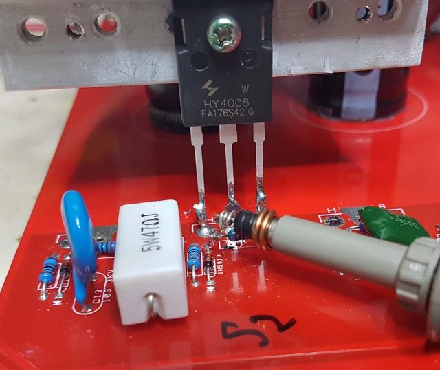 The diff. probe technique is very, very dodgy. 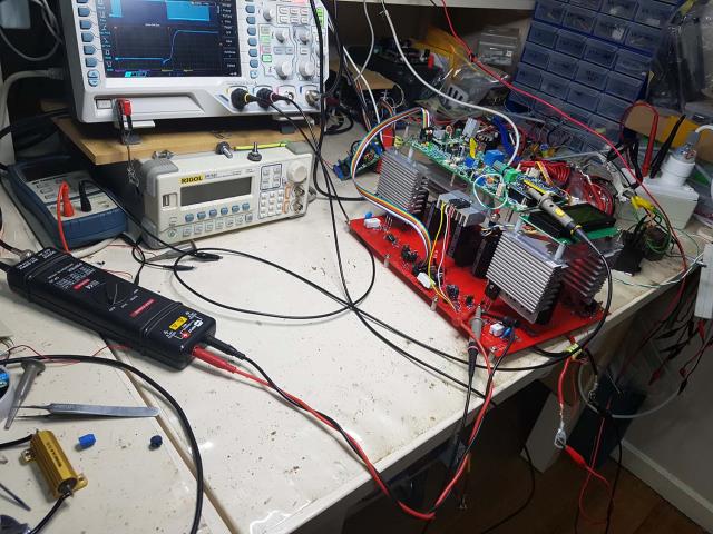 and the common mode test you wanted 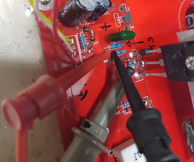 But the results speak for themselves. Dark Blue is from the Pintek DP-25, at 20x. Here are the two samples, one from both clips on one end of the 10R and the next with both clips on the other end. 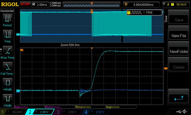 and  Here I show the proper gate voltage, with good probe tech, on top of that which I get from the differential probe with the clips on each of the 2 wires There are differences but it's not too bad. 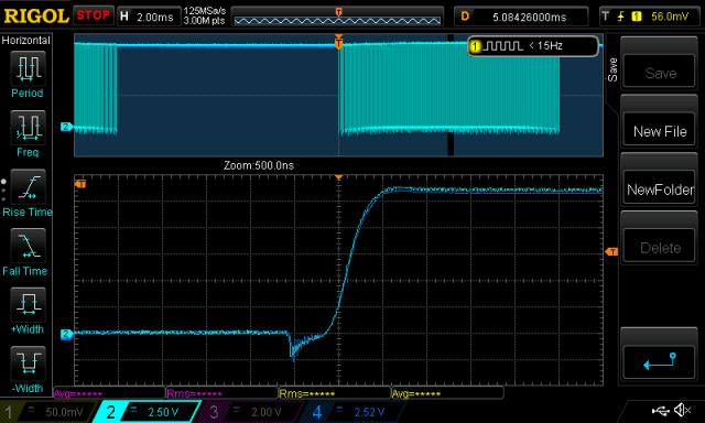 For sure there will be EMI everywhere. I try to concentrate on the gross issues and I feel I can easily reproduce them upon request. Lastly, here is the low and high side gate voltages, to show the high side's behavior during that curious negative dip in the low side Vgs. Dark Blue is high side, Light Blue is low side. All high side measurements use the DP-25. 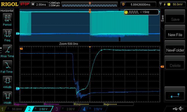 This is the same thing but with both high side leads shorted on the gate end of the 10R resistor. 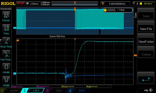 I suspect better results could be obtained from the DP-25 with a custom shielded probe built from a cheap CRO 10x probe and 2 banana plugs. Twisting the two leads together helps a bit, but things could be better. wronger than a phone book full of wrong phone numbers |
||||
| Warpspeed Guru Joined: 09/08/2007 Location: AustraliaPosts: 4406 |
One trick to achieve better high frequency common mode rejection, even with an ordinary single ended CRO probe, is to wrap a few turns of the probe lead through a very high permeability ferrite toroid. This causes the whole probe lead act like a broad band common mode transformer. It also adds series impedance to the ground lead at higher frequencies which will reduce any heavy circulating ground currents between CRO and what you are testing. Most large toroids are crappy low permiability powdered iron and pretty useless for this. If you can find a suitable core, this can work really well. This may even add some extra high frequency CMRR to your new magic differential probe. No harm in trying ! Cheers, ĀTony. |
||||
| The Back Shed's forum code is written, and hosted, in Australia. | © JAQ Software 2026 |