|

|
Forum Index : Electronics : Various aspects of home brew inverters
| Author | Message | ||||
Revlac Guru Joined: 31/12/2016 Location: AustraliaPosts: 1239 |
I too have been thinking about this. Most of the generators will be running at a bit higher voltage then we set our inverters, so that may have some limit/control on the amount to be backfed through the inverter to the batteries. There is going to be a bit of field testing involved to see how things work  . . Cheers Aaron Off The Grid |
||||
| Tinker Guru Joined: 07/11/2007 Location: AustraliaPosts: 1904 |
Once they are synced the AC generator just becomes a power source running at the frequency of the inverter. While driven by its motor the generator will contribute power to the inverter. If the motor is turned off (ran out of fuel) the AC generator will continue to run in sync (as a motor) but taking power from the inverter to do so. Of course, if the inverter does not have enough power to drag the generator & dead motor things might get interesting... Its a little different with the grid tie inverter. This senses input power from the solar panels and, if not sufficient, cuts syncing out via relays. I suppose one could fit fuel tank level sensing and have this cut the syncing relay if the whole kaboodle is to run unattended. Klaus |
||||
| tinyt Guru Joined: 12/11/2017 Location: United StatesPosts: 556 |
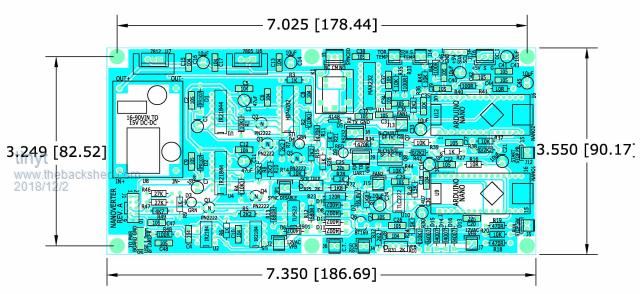
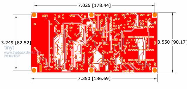
Since there are no more change requests, here is minor revision on the schematic now locked at Rev A. 2018-12-02_035039_nanoverter_Rev_A.pdf 1. Placed values on resistors that are TBD or SEL. 2. Changed Q5 to BJT. 3. More informational notes. Finally a PCB file(s). Connections were auto-routed, it is the only one I can do. I think it is OK since the operating frequency is low (23kHz). I tried to match PCB outline dimensions and corner mounting holes with those on the Clockman/oztules control PCB.   Will post live files next. |
||||
| tinyt Guru Joined: 12/11/2017 Location: United StatesPosts: 556 |
Here are the live gerber files.2018-12-02_044343_NanoverterPCB.zip 1. Schematic pdf 2. Gerbers (zip) 3. Fab notes. 4. BOM No guarantees that it is error free. Those who have the courage can order the pcb to experiment. Maybe for now have it made using 1 Oz copper. |
||||
| Clockmanfr Guru Joined: 23/10/2015 Location: FrancePosts: 437 |
Hi tinyt, Nicely done, a Very interesting development. I will experiment with this board in the near future. Thanks. Everything is possible, just give me time. 3 HughP's 3.7m Wind T's (14 years). 5kW PV on 3 Trackers, (10 yrs). 21kW PV AC coupled SH GTI's. OzInverter created Grid. 1300ah 48v. |
||||
| poida Guru Joined: 02/02/2017 Location: AustraliaPosts: 1464 |
Tinyt and all, I have discovered a problem. It relates to the displayed AC output voltage. Nano1 is designed to increase or decrease PWM % to maintain the AC output to equal the set point. The set point is approx 3.0V. So nano1 program tries to make VFB = 3.0V. So far so good. We adjust AC output voltage by changing the voltage divider R31 trim pot on page 2 to suit the desired AC voltage as measured on the toroid secondary. VFB signal is connected to nano1, for driving the AC output. It also is connected to nano2, used to display the output voltage. The problem is, no matter what calibration we give nano2 for displayed AC voltage, we will always see the same displayed voltage FOR ALL AC OUTPUT VOLTAGES SET BY R31 trim pot. Nano1 does a good job of doing what is needed to make VFB = 3.0V It will always = 3.0V, all things going well, no matter the AC output voltage as measured on the toroid secondary. Solution: We need a separate AC input for nano2, it can not be the existing VFB. Could I suggest we run, from positive terminal of C30, a line to a 1/3 voltage divider, then RC LP filter, then into nano2 ADC channel 0, pin 19. Maybe aim to produce 4.0V here when the output voltage is 240V AC. This will be a fixed voltage divider, giving a fixed fraction of the AC output voltage. We will continue to use the variable divider (R31) to set the inverter output set point as usual. I don't know if we need to bother with opamp buffering this. It's up to you. We call this VSAMP for voltage sample? wronger than a phone book full of wrong phone numbers |
||||
| Tinker Guru Joined: 07/11/2007 Location: AustraliaPosts: 1904 |
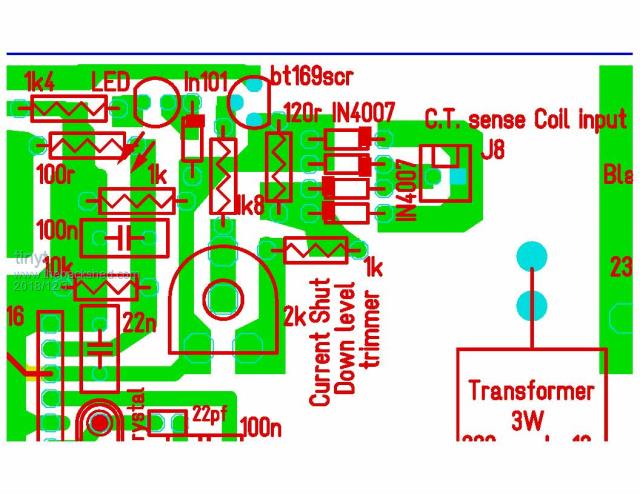
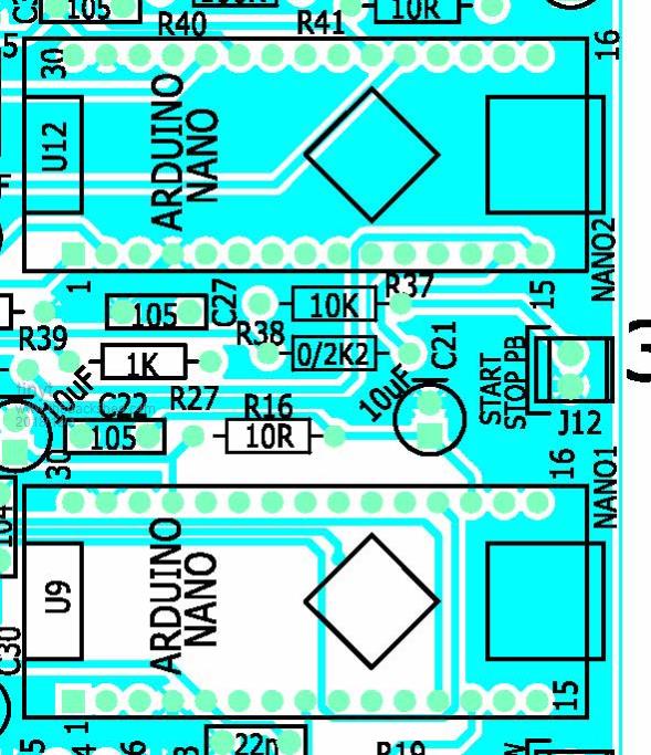
Thanks tinyt, those added comments are very helpful. I will re draw your circuit minus the parts that are not required for my control board. Hopefully I can fit it onto one page so its a bit easier when laying out my board. A comment or two; should R23 (120R) not be located directly across the CT terminals? It may be helpful if nano 1 and nano 2 are clearly marked so on the PCB to avoid confusion. They were referred by that throughout this topic, making the U9 & U12 identification meaningless. Also, the 6 little boxes (M1 - M6) on page 1, bottom right, have me wondering what they represent? Klaus |
||||
| wiseguy Guru Joined: 21/06/2018 Location: AustraliaPosts: 1267 |
Tinyt, R17 needs to be ~390R by my calculations. For ~ 5V to be on SCR_SD whem active, there are 4 current paths bleeding current from SCR_SD, R8, R10, R21 & R28, they total ~ 12.5mA if SCR_SD is 5V. Poida, can the V adjust pot be after the active filter ? The input of the filter would be a normal voltage divider ~ say 12V in 3 or 4V out. The pot connects to the filter out & drives the VFB pin, the output of the filter before the pot can also be read by an analog input and is proportional to Vout. Obviously a gain value has to be selected for the Vout analog measurement calibration. (The output voltage measurement and the VFB adjuster both receive the filtered voltage) If at first you dont succeed, I suggest you avoid sky diving.... Cheers Mike |
||||
| tinyt Guru Joined: 12/11/2017 Location: United StatesPosts: 556 |
The connection of the 120R burden resistor is a straight copy from clockman/oztules gerber:  But I think your suggestion is better, it eliminates the current flowing thru the 120R from heating the diodes and affecting the trigger voltage of the SCR. Rev B schematic/PCB will have the change. The picture of the pcb top is probably not too detailed, here is a close up showing silkscreen "NANO1" and "NANO2" close to the USB connectors at the PCB board edge:  But I think you are also correct, the arduino nanos are not chips but modules. Rev B schematic/PCB will have the change. M1 - M6 are mounting holes (3.8mm hole, 6.6mm pad), I add them in the schematic to account for all footprints. I will add the info in the rev B schematic. |
||||
| tinyt Guru Joined: 12/11/2017 Location: United StatesPosts: 556 |
Will change R17 to 390R. The way I understand it the AC-out - VFB - code - PWM - mosfet/toroid is a closed loop system. So per poida, "It will always = 3.0V, all things going well, no matter the AC output voltage as measured on the toroid secondary." Maybe if we mimic the EG8010 to PWM shutdown and also report VFB over-voltage/under-voltage in case of a component failure. We can use the PWM-ON led to flash for this condition. To do this we will need to change the LED connection to one of the un-used DIO of nano1 and support it in code. |
||||
| wiseguy Guru Joined: 21/06/2018 Location: AustraliaPosts: 1267 |
The node that will always be 3V is the wiper connection of the pot. The end of the pot fed from the filter/transformer/whatever will always have the correct output voltage measurement information - put a multimeter on the high end of the trimpot and adjust the wiper setting and see for your self. Its not a critically important point but should be understood. If the Pot wiper is at the maximum end for the correct output voltage, the maximum end will be 3V. If the pot wiper is at the minimum setting end for the correct output voltage the minimum pot end will be at 3V. Therefore the maximum end will be much higher than 3V (I am assuming ohms law still works). (If it didnt contain the output voltage information then it would not be a closed loop allowing adjustment of the output voltage) If at first you dont succeed, I suggest you avoid sky diving.... Cheers Mike |
||||
| tinyt Guru Joined: 12/11/2017 Location: United StatesPosts: 556 |
I think I understand it better now. Thanks wiseguy. |
||||
| poida Guru Joined: 02/02/2017 Location: AustraliaPosts: 1464 |
Correct: It is a closed loop system. Right now, with my test system using a cheap Uno clone for nano1, the latest nano1 code results in the inverter maintaining the "3V" as 2.78V This is not and never will be a problem. I can adjust one line of code in nano_1_v3_sync_pid to bring it up to 3.0V look for ac_setpoint = 0.56; and change it to ac_setpoint = 0.604; // 0.56 * 3.0/2.78 If we are using a 12V AC transformer, this will put something like 12V RMS on it's secondary, or nearly 17V peak to peak. This then is rectified by the bridge, and allowing for 2x diode drops of about 1V, we probably will see 15V DC across C30, a 4.7uF cap. Wiseguy proposes putting this into the TLC2272 opamp. The specs for this opamp say max supply voltage is 8V and inputs must be within supply volts and -0.3V I don't like that. Maybe replace R31 trimpot with a fixed voltage divider, to take 16V to 4V. Maybe a 6.8K and 2.5K combo, to give 4V This 4V goes into the opamp input, and it also becomes VSAMP, to lead into nano2 ADC channel 0. We produce VFB via a trimpot placed at the output of TLC2272, pin 7 which will trim down the 4V to approx 3V. This gives us ample scope to set the AC output voltage to anything we want. This is my preferred change to the circuit. Can we assume the opamp will never get more than 5V input into pin 3? It is an important question to answer. Should the opamp get an overloaded input, will it survive? The inverter then may or may not get a useful VFB with a now compromised opamp and so PWM duty cycle % will go to maximum or minimum. This will be a bad thing, and depending on your toriod turns ratio, you will have 260V AC or higher powering the loads. Probably not a lot higher since the toroid will become close to saturated and become a near short to the MOSFET bridge. If I was doing the circuit (after thinking of the above failure mode) I would not use an active filter on VFB, to remove this risk completely. Since it is there, could I add a 5V TVS across the opamp input, to opamp ground too? wronger than a phone book full of wrong phone numbers |
||||
| tinyt Guru Joined: 12/11/2017 Location: United StatesPosts: 556 |
It is a closed loop system. Right now, with my test system using a cheap Uno clone for nano1, the latest nano1 code results in the inverter maintaining the "3V" as 2.78V This is not and never will be a problem. I can adjust one line of code in nano_1_v3_sync_pid to bring it up to 3.0V look for ac_setpoint = 0.56; and change it to ac_setpoint = 0.604; // 0.56 * 3.0/2.78 If we are using a 12V AC transformer, this will put something like 12V RMS on it's secondary, or nearly 17V peak to peak. This then is rectified by the bridge, and allowing for 2x diode drops of about 1V, we probably will see 15V DC across C30, a 4.7uF cap. Wiseguy proposes putting this into the TLC2272 opamp. The specs for this opamp say max supply voltage is 8V and inputs must be within supply volts and -0.3V I don't like that. Maybe replace R31 trimpot with a fixed voltage divider, to take 16V to 4V. Maybe a 6.8K and 2.5K combo, to give 4V This 4V goes into the opamp input, and it also becomes VSAMP, to lead into nano2 ADC channel 0. We produce VFB via a trimpot placed at the output of TLC2272, pin 7 which will trim down the 4V to approx 3V. This gives us ample scope to set the AC output voltage to anything we want. This is my preferred change to the circuit. Can we assume the opamp will never get more than 5V input into pin 3? It is an important question to answer. Should the opamp get an overloaded input, will it survive? The inverter then may or may not get a useful VFB with a now compromised opamp and so PWM duty cycle % will go to maximum or minimum. This will be a bad thing, and depending on your toriod turns ratio, you will have 260V AC or higher powering the loads. Probably not a lot higher since the toroid will become close to saturated and become a near short to the MOSFET bridge. If I was doing the circuit (after thinking of the above failure mode) I would not use an active filter on VFB, to remove this risk completely. Since it is there, could I add a 5V TVS across the opamp input, to opamp ground too? Will do. The only thruhole TVS I can find with voltage rating close to 5V is 1N6373 (Vbr = 6V, Vclamp = 7.5V) I am not sure if this PN is readily available. May be a 1N47xx zener diode will work. At any rate I can add a DO-41 footprint and experiment what part number to use. Can I also transfer the PWM-ON Led connection to nano1 pin 15? Maybe VSAMP should also be monitored by nano1. Let me know. |
||||
| poida Guru Joined: 02/02/2017 Location: AustraliaPosts: 1464 |
Tinyt: agree, a 5V zener would be fine. Maybe only the Mouser part NZX4V7C,133 which is a 4.8V zener, through hole. The specs of TLC2272 make it clear that inputs may never exceed Vdd, which is 5V at the moment. So 5.1V zener is not good enough. We need to keep it at or below 5V. Recommended input voltages are Vdd - 1.5V, or 3.5V to ground. And I have been saying "let's make the voltage divider produce 4V" It will be trivial to transfer PWM_ON led to pin15 (D12) in code. This will not result in any performance issues. VSAMP only makes sense for humans to view the output voltage, and nano2 to perform actions appropriate to low voltage. I think nano1 does not need to know output voltage, just VFB for the closed loop control. wronger than a phone book full of wrong phone numbers |
||||
| tinyt Guru Joined: 12/11/2017 Location: United StatesPosts: 556 |
agree, a 5V zener would be fine. Maybe only the Mouser part NZX4V7C,133 which is a 4.8V zener, through hole. .... It will be trivial to transfer PWM_ON led to pin15 (D12) in code. This will not result in any performance issues. VSAMP only makes sense for humans to view the output voltage, and nano2 to perform actions appropriate to low voltage. I think nano1 does not need to know output voltage, just VFB for the closed loop control. OK, will revise the schematic for the NZX4V7,133 zener and PWM_ON led connection. On the VSAMP, I was thinking that should any component in the closed loop malfunction and cause out of range AC output, then nano1 using VSAMP out of range value can stop the PWM and blink the PWM_ON led. |
||||
| Solar Mike Guru Joined: 08/02/2015 Location: New ZealandPosts: 1203 |
If you wish to protect the input pin 3 of the TLC2272, replace the connection P3 to the pot with a 15K resistor and connect a silicon diode between P3 and +5v rail. Leave C28 in place, this will just add another pole to the filter. Cheers Mike |
||||
| poida Guru Joined: 02/02/2017 Location: AustraliaPosts: 1464 |
I'm not sure I like that, we need to protect > 5V excursions at any frequency appearing on the inputs (either inverting or noninverting). Would your idea prevent +5V coming INTO the opamp? given: the opamp Vss = 5V in this design. TI specs say inputs must not have more than Vss on inputs wronger than a phone book full of wrong phone numbers |
||||
| poida Guru Joined: 02/02/2017 Location: AustraliaPosts: 1464 |
On the VSAMP, I was thinking that should any component in the closed loop malfunction and cause out of range AC output, then nano1 using VSAMP out of range value can stop the PWM and blink the PWM_ON led. That's a nice idea, I need to have a think on this, in particular, how much time will be spent checking for this condition. At first glance, I think not much time and so it's very possible. I will want to confirm later with you the behavior of this added code to check if I am on the same page... wronger than a phone book full of wrong phone numbers |
||||
| Solar Mike Guru Joined: 08/02/2015 Location: New ZealandPosts: 1203 |
appearing on the inputs (either inverting or noninverting). Would your idea prevent +5V coming INTO the opamp? given: the opamp Vss = 5V in this design. TI specs say inputs must not have more than Vss on inputs As there are no inbuilt protection diodes according to the spec sheet, placing one externally and limiting the current that could flow on higher than +Vcc inputs (15K resistor), is the accepted way of protecting an input. I have been using this method over the past 30 years of designing with Op Amps and had no issues with it. Using zenners and the like, affect the input signals due to their inherent leakage currents, so not recommended. Perhaps if one is paranoid the build notes should say, move the pots wiper to the 0v end prior to applying power, then adjust it to 3v setting. Cheers Mike |
||||
| The Back Shed's forum code is written, and hosted, in Australia. | © JAQ Software 2026 |