|

|
Forum Index : Electronics : all home built solar system
| Author | Message | ||||
| wiseguy Guru Joined: 21/06/2018 Location: AustraliaPosts: 1267 |
1000 pages?? I wont be discussing this further after this post. I always only use 12V for Mosfet drive. I always use a 4R7 (or sometimes smaller) with parallel diode, but depending on application I may not install the speed up diode. In my inverter each group of 4 x HY4008 use just ~ 15mA of average drive current. With all 16 FETs being driven the total including all the wasted power of negative bias sucks a measly total current of just 58mA from the 12V supply, when including the idling current of the 4 x opto driver ICs and the small isolated dc to dc converter it was 98mA total. I don't think this energy level will overstress the drivers too much. My inverter Gate Waveforms are reproduced here for interest. Please note the 100nS time scale and the total absence of gate bounce and ringing & oscillations. For interest here here is how my waveforms used to look before finding the cure that solved both my 12V & 48V inverter issues. Edited 2021-05-01 09:02 by wiseguy If at first you dont succeed, I suggest you avoid sky diving.... Cheers Mike |
||||
| Haxby Guru Joined: 07/07/2008 Location: AustraliaPosts: 423 |
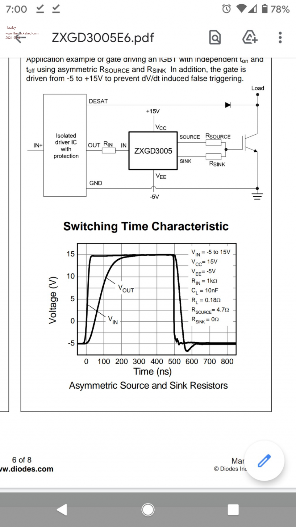
This is a great discussion guys.... I had a heap of problems driving my IGBTs and ended up "solving" the gate bounce issues with 82nf caps on the gates. Not an elegant solution. I'm going to re-visit my solution based on the info I have picked up here. To save re-manufacturing some large PCBs I want to make up some very small piggyback boards to fit between the existing gate driver chips and the igbt gates. The ZXGD3005 looks good. It's a totem pole 9A driver with separate source and sink pins. I think Solar Mike recommended them in another thread. Wiseguy, do you suggest 4R7 resistors for both charging and discharging the gate? What sort of inductor do you use for the gate lead?  |
||||
| poida Guru Joined: 02/02/2017 Location: AustraliaPosts: 1464 |
Mike, my results with -5V bias is here It was a power board that used IR2110 to drive the gates, not an onboard BJT totem-pole The test pulled Gate low to -5V but still the high side oscillated. Of course there is much more to this. (A bit of my Hacker mentality follows) The home inverter is near 2 years old. If it has ran for 1/2 that time due to low input voltage cut-off then that is 1 year continuous. how many switch cycles? 365 days x 24 hours x 3600 seconds x 20,000 PWM rate = 6.3E10 cycles, and 1/2 that for each half bridge. 3.2E10 switch on/off events with this shoot through. I'd love to use some simple changes to control this but right now I am happy with how it runs. The air compressor start up test I did with it put 11kW through 3 FETs. This has them close to SOA limits. The shoot through must reduce the safe margin further. It's only a matter of time.. My benchmark for inverter longevity is the 3kW Victron that lasted 2 years. It failed when under 500W load. Not an 11kW event. 2 years so far with a board that costs $50? That delivers 3kW regularly? 4 FETs per side too so it's easy to repair and cheap too. I can live with that. wronger than a phone book full of wrong phone numbers |
||||
| wiseguy Guru Joined: 21/06/2018 Location: AustraliaPosts: 1267 |
Haxby, I couldn't do a better job describing IGBT's than these 2 application notes I will link to: App note 1) Infineon-EiceDRIVER-Gate_resistor_for_power_devices-AN-v01_00-EN.pdf App Note 2) AN-7003_Gate_Resistor-Principles_and_Applications_rev00.pdf Warp and Solar Mike have a lot more experience with IGBT's so I would rely on their help and the App notes to find your solution. As you will see from the App notes larger gate resistors than MOSFET's use are common. The problem and solutions we are discussing here are less relevant than with IGBTs they are a bit different when it comes to problems, causes and solutions. Edited 2021-05-01 16:56 by wiseguy If at first you dont succeed, I suggest you avoid sky diving.... Cheers Mike |
||||
| wiseguy Guru Joined: 21/06/2018 Location: AustraliaPosts: 1267 |
Peter, the negative bias and the ringing are totally unrelated topics. In my career if I ever took a short cut and put something in production prematurely it inevitably would come back and bite me in the ass. This has caused me to be very cautious, pessimistic and strive to get it right from the get go - almost to the point of obsession. When I made my inverter board Rev0 - that has exceeded my expectations to date - I had read hundreds of posts here and had a few odd arguments with others along the way and built my board the way I believed it would perform best and that meant not following a Mad/Oz style build (or thanks to you the dreaded EGS002) but going with my experience and intuition and drawing from all the good things I read that resonated with my thinking. I did say from the outset that I did not want to build an inverter power board that would interface to an oz/mad controller as I did not believe the approach was right or best and considered that I would have an existing Achilles heel if I did. The ringing that I found with each prototype I played with always responded and went away with a drain ferrite bead on the lower side FET's. But I had a totally different power stage. I used low impedance opto drivers with fast high current transistor buffers all on the same PCB avoiding the dreaded ribbon cable fiasco. All gates drives had a 2R2 and around 80mm of total track length. I use a ribbon cable that carries opto drives in inverse parallel and I have isolated optos & power supplies the only common connection is ground which was only needed for measuring the input voltage. So when I see an issue like the gate bounce I observed, I think maybe I should pull my head in and just be an observer. We are fighting two different animals in the end. You might build a hundred the way they are and they will all work properly on the other hand......I dont profess to know that answer only time will tell. There is no argument that it works but perhaps there is not a large enough sample to draw all the right conclusions from yet. I did not mean to say it was shoot through only that it was headed that way and how much space was there till it became shoot through. If it (gate bounce) could be lessened surely it would only be a positive result ? Edited 2021-05-01 17:31 by wiseguy If at first you dont succeed, I suggest you avoid sky diving.... Cheers Mike |
||||
| poida Guru Joined: 02/02/2017 Location: AustraliaPosts: 1464 |
yup. Redesign the gate drive from the start. Probably the way to go. Earlier today I was dreaming of a one opto-gatedrive IC per FET design. All optos have tight bypassing caps and short as can be traces. And something like 5R gate resistors. Maybe gate shutdown diodes. SMD all the way. It's do-able. loop path lengths of the order of 10mm and probably less. I wonder how that would go... oh, and a +/- 12V floating supply. For a standard inverter power board I need 3 +/- 12V supplies. so that's $36 for the Recom RE1212 with +/- 12V output Maybe get away with 2. Optos for each FET $3.60 in packs of 5 if using FOD3182 Need 16, buy 20 in packs of 5. Prob, cheaper elsewhere than RS.. so a 4 x 4 FET power board will be $72 for the 3 Amp optos and $36 for the iso supplies I can afford that test. Give me a bit of time. heh, 10mm long loop. "yer dreamin mate.." more like a lot longer. Edited 2021-05-01 18:58 by poida wronger than a phone book full of wrong phone numbers |
||||
| Solar Mike Guru Joined: 08/02/2015 Location: New ZealandPosts: 1203 |
Poida, if I was designing something like what you are describing, perhaps use these tiny SOT23-5 4 amp drivers, one per mosfet; common their inputs and drive from an opto isolated driver like the FOD3182 or similar. You can mount each within mm from the mosfet gate. A coincidence, I'm actually designing a pcb with 24 of them right now - UCC27519 non inverting, one per mosfet. I have used the ZXGD3005 in the past but as they are emitter followers they don't switch rail to rail, the UCC27519 is the same size but with more options and perhaps better. Cheers Mike Edited 2021-05-01 18:57 by Solar Mike |
||||
| Haxby Guru Joined: 07/07/2008 Location: AustraliaPosts: 423 |
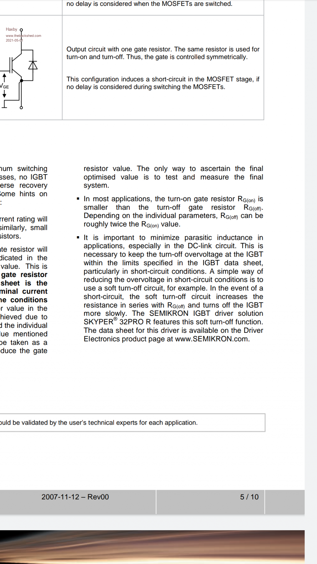
Wiseguy: that was a good read. Basically sums it all up nicely. Particularly the dv/dt and di/dt issues, which are amplified when switching higher voltages. One thing that surprised me is in the second link it says that the "on" gate resistor is usually lower value than the "off" resistor. In my experience it is the opposite, though most designs I see refer to MOSFETs not IGBTs. Any insights on this?  Poida: have a look at the Hi-Link dc-dc range if cost is an issue. |
||||
| Warpspeed Guru Joined: 09/08/2007 Location: AustraliaPosts: 4406 |
If I was living in a nightmare world where I had to drive ten mosfets in parallel, that is how I would probably do it. One driver chip per mosfet, up close and personal to each mosfet. Or one driver and two mosfets with a symmetrical layout, almost as good. Driving any more than two mosfets with one driver, and it all becomes vastly more difficult and trouble prone. The trick then, is how to drive the inputs of the ten individual gate driver chips. That could be done by use of a transmission line, correctly impedance matched at both ends so there will be no reflections or ringing. Each driver chip input can be distributed along the transmission line, because the input impedance will be quite high compared to the impedance of the transmission line. The whole thing could be driven by a single opto source if galvanic isolation is required, and it should be. This technique of driving multiple devices in parallel is called a "distributed amplifier" and is quite commonly used at microwave frequencies. It also works at much lower frequencies where you need nice clean very fast edges without any reflections or ringing. https://en.wikipedia.org/wiki/Distributed_amplifier Cheers, ĀTony. |
||||
| wiseguy Guru Joined: 21/06/2018 Location: AustraliaPosts: 1267 |
Mike I bought some ZXGD3005's but I haven't used them - they intimidated me - they were bordering on invisible & even with their generous current ratings I couldn't bring myself to design them in as although I can and have designed smd for years, when I cant rely on pick and place machine and a reflow oven it all gets too hard for my old eyes. ....some Hours later - we had guests tonight and I missed the party here :( I decided to be a bit of a trailblazer and recently designed a cascade-able power bridge stage using pretend optocouplers, the capacitively coupled isolators. They looked to be an answer to a Maidens prayer. They are the UCC53##UCC5310.pdf series of opto isolators. only one in the series has an UVlockout of 8 volts (the one I am using with 12V) the others have a UVLO of 12V and need ~ 15V supply. They have a variety of flavours and drive currents up to typ 10A+, handling split pull up/down resistors, negative bias, miller clamp etc. Their common mode transient immunity starts at 100KV/uS and their small propagation delays and tight part to part skew is attractive & they cost around a whole $2.50 - $3 from digikey. They are in a SOIC8 but I forgive them that transgression and have designed a small SOIC8 to DIP8 adaptor that maintains good I/O isolation. IF they behave the way I hope they will, I might just move away from optocouplers. If at first you dont succeed, I suggest you avoid sky diving.... Cheers Mike |
||||
| wiseguy Guru Joined: 21/06/2018 Location: AustraliaPosts: 1267 |
Now I want to buy into the how do we do this best discussion. I define best as, fit for purpose, minimum complexity, low part count, low cost, reliable, easily serviceable, (with a good design hopefully that wont be often) and can be built by a typical home constructor by following the plan and not having access to SMD tools. I applaud Solar Mike in his approach with separate buffers, that is somewhere between his perfect world scenario and Warps nightmare world. I would like a camp somewhere midway between the two. Now I ask hopefully a relative question, what are we trying to achieve by presenting a perfectly matched to the nano second on and off command to our paralleled MOSFETs ? It is relevant here to look at a data sheet, one where they have been brave enough to provide typical switching behaviour of a brand name MOSFET - not many manufacturers give this data and only show a typical value which is almost meaningless to us. Here is the datasheet FDH055N15A.PDF Now go to page 3 and look at the switching times (which dont state a minimum either) and see that the spread from typical to Max is greater than 1:2 (Poidas 1=2 is starting to look more relevant  ). So we got our perfectly matched Gate signals all arriving at the same nanosecond and watch our MOSFETs stuff it up grandly with their different spread of switching behaviour times. ). So we got our perfectly matched Gate signals all arriving at the same nanosecond and watch our MOSFETs stuff it up grandly with their different spread of switching behaviour times.If we look at the circuit we are trying to control, it is switching an inductive load, current is (should be) at its lowest level at the turn on event. I would suggest maybe 1 MOSFET could safely handle that at this point, within say 200 nanoseconds all Mosfets should now be shouldering the load on their way to some maximum current & before saturation. Now we turn them off and again within 200nS from fastest to slowest the FETs are now all off. Without doing a heap of maths I reckon that again one FET shouldering that current level for 200nS is probably fine also. In my opinion, what is critical is having an inductor that will never saturate under any conditions of normal operation, or only saturates softly. Ensure that there is no tendency for Gate bounce (heading for unintended conduction or shoot through)). Ensure there is no tendency for oscillation of the Gate/Drain in any of the bridge quadrants and maybe you have a better chance at a long life. Although I haven't thrashed my Inverter as much as I would like it appears to be strong and free of any bad tendencies to date. IF I was tempted to try to improve its performance, I would not change the 1 optocoupler and buffered common gate drive that I used, but perhaps dividing the bridges to 4 x Highside/Lowside Fet nodes that drive 4 smaller chokes that are commoned on their output side. This would force better current matched sinewave signals whilst each pair of MOSFETs shoulders its part of the power without worrying so much about the exact nanosecond timing of all the other pairs - no slow FET then has to shoulder a bulk current, only 25% of it, assuming a 16 FET Power stage. To save me drawing it out, essentially just imagine a single 4 FET bridge power stage with an output choke. Couple 3 more similar circuits and sum all the choke outputs and we have a much more nicely sharing current scheme ? All of the power quadrants are still driven from the same common opto/buffered gate drives of the original output stage. I think that's enough for now.... patiently waiting to be shot down in flames....... If at first you dont succeed, I suggest you avoid sky diving.... Cheers Mike |
||||
| wiseguy Guru Joined: 21/06/2018 Location: AustraliaPosts: 1267 |
Peter, I advise don't rush into a new design just yet & let the waters settle a bit and see what we can collectively agree to and come up with. I think there was/is a trend towards over engineering the inverter at this stage, of course all with the right intentions but there may be other paths to a simpler but more robust design. For interest why not tack some 4.7R resistors in parallel with the 10 Ohm gate drive resistors on your board - maybe just on one or both of the low side FETs and look to see if the gate bounce issue is improved (less). Afterwards if further inspired also try a ferrite bead on each of the Drains of the low side FETs - just on one side and see if the tendency towards oscillation has gone (obviously on that side....)? I am assuming the FET's are insulated from each other & the heatsink. If this is too hard to achieve don't go to the trouble. If at first you dont succeed, I suggest you avoid sky diving.... Cheers Mike |
||||
| poida Guru Joined: 02/02/2017 Location: AustraliaPosts: 1464 |
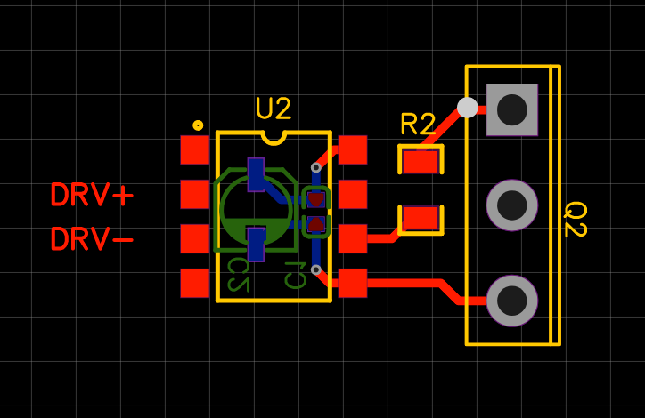
A compact layout could be like this:  isolated opto inputs 0 to +12V and -12V to +12V supply possible. I intend to use jumpers to permit selection between the 2 drive options short gate drive traces but can be built by me and my bad eyesight. wronger than a phone book full of wrong phone numbers |
||||
| Haxby Guru Joined: 07/07/2008 Location: AustraliaPosts: 423 |
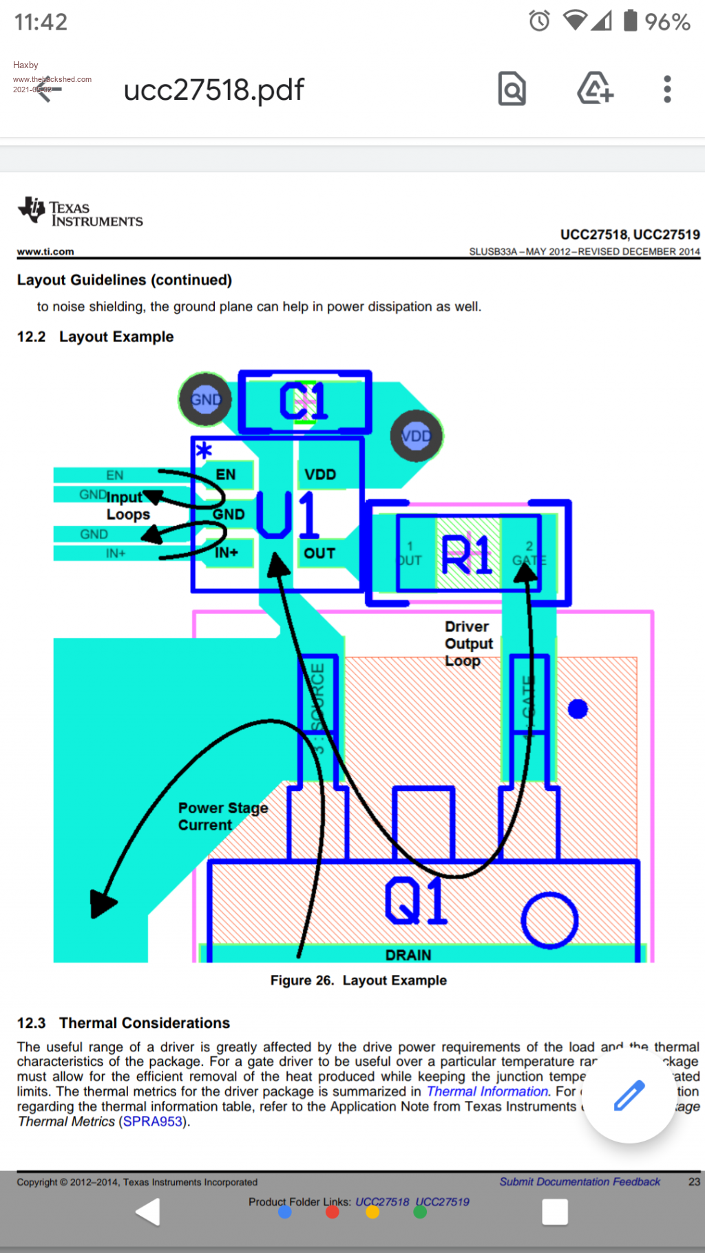
Double sided SMD boards will certainly scare away most hobbyists. Here is the example layout of the ucc27518 Solar Mike referred to: Single side loaded components and as big a tracks as you can afford   |
||||
| Haxby Guru Joined: 07/07/2008 Location: AustraliaPosts: 423 |
Poida what chip is that? |
||||
| poida Guru Joined: 02/02/2017 Location: AustraliaPosts: 1464 |
Haxby, it's the TLP350 in PDIP SMD package. Chosen at random. Obviously better/smaller choices there. I want isolated input signals so it's something like that and not the UCC27519 even though this chip is tiny and allows tighter loops. wronger than a phone book full of wrong phone numbers |
||||
| Solar Mike Guru Joined: 08/02/2015 Location: New ZealandPosts: 1203 |
Yeah they are pretty tiny, I just use a hot air gun to solder them, and a pair of x4 reading glasses, not too much of an issue really. Have used the UCC5350SB 5 A and 5 A Split Output with 8 V UVLO, on many designs, they are an excellent replacement for older tech opto's. One could easily drive two parallel mosfets. Your idea of using multiple 4 mosfet stackable bridge modules combined together via their output inductors makes a lot of sense, it effectively prevents problems of getting a big bunch of 4 - 6 parallel mosfets to work together. If you want more output power then plug in more modules, brilliant. I will have a re-think about the board I'm currently working on. Cheers Mike |
||||
| poida Guru Joined: 02/02/2017 Location: AustraliaPosts: 1464 |
I am looking at Si826x range of drivers. One of them can do 4A peak output drive current. They have internal resistances of about 2.5 and 0.8 Ohms for source and sink respectively. This works out nicely so that if I use an external gate drive R of 2.5 then I get about 5R for source (pulling Gate high) and 3.3R for sinking Gate current/pulling it down to Source. The part has good common mode rejection, 5kV isolation, needs about 10mA to drive the "LED". There is no LED. It's emulated. The footprint is tiny and suits this application well. SDIP6 with Vcc, output and Ground all on one side. And fast too. wronger than a phone book full of wrong phone numbers |
||||
| Warpspeed Guru Joined: 09/08/2007 Location: AustraliaPosts: 4406 |
That Si8296 is a good bit of kit, very nice find Peter. Close delay matching between pieces too, which can be a problem with the real optically isolated drivers. Cheers, ĀTony. |
||||
| Haxby Guru Joined: 07/07/2008 Location: AustraliaPosts: 423 |
It's good to live in a world where we are spoilt for choice. That UCC5350MC looks like the answer to my particular prayers. The Miller clamp in particular will be invaluable. Poida have you considered driving the gate negative? The component count increases by 1 single zener diode and the choice of dc-dc converter could be changed to a 15v or even 24v type. |
||||
| The Back Shed's forum code is written, and hosted, in Australia. | © JAQ Software 2026 |