
|

|
Forum Index : Electronics : Various aspects of home brew inverters
| Author | Message | ||||
| noneyabussiness Guru Joined: 31/07/2017 Location: AustraliaPosts: 527 |
Hey poida, i tried replying to you but your inbox is full... I think it works !! |
||||
| poida Guru Joined: 02/02/2017 Location: AustraliaPosts: 1464 |
use an op-amp to drive the MOSFET Gate. Build this on the breadboard, and you can just plug in each HY4008 and test. 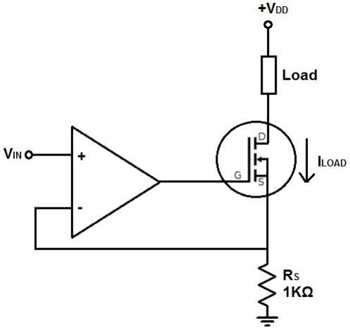 Vin will control the voltage across the 1K resistor. Since the resistance is nearly constant, Vin now controls the current, when the op-amp is doing it's voodoo. 1V at Vin will mean 1V across the 1K resistor, or 1mA. The HY4008 specs show they test Vgs(th) at 250uA. Maybe use a 5KR for Rs, to increase the sensitivity. Produce Vin by using a 1KR potentiometer, and measure Vin with any DMM. I have made the above circuit, with a 50R resistor on the op-amp output, in series with the Gate. This is to help prevent oscillation. The circuit I built uses 10W 0.5R current sense resistor instead of the above 1KR. It is used as a constant current DC load, and works perfectly well over 150W. I used the cheap and available everywhere LM 258 op-amp since it goes quite close to ground on it's output. I would expect nearly any op-amp will do the job. wronger than a phone book full of wrong phone numbers |
||||
| poida Guru Joined: 02/02/2017 Location: AustraliaPosts: 1464 |
wronger than a phone book full of wrong phone numbers |
||||
| wiseguy Guru Joined: 21/06/2018 Location: AustraliaPosts: 1267 |
I wonder if anyone told this to the core memory guys - never say never  I may not design beads into circuits generally but am very happy to fit them or prepare for them not only for EMC but to cure abhorrent circuit behaviour. I cant really see much difference in providing for an axial inductor or using a wire and bead if value is not that critical. However choosing random beads from a tray of different shapes and sizes is not what I do. I use Fairite or Neosid or similar traceable parts with repeatable results. Tony, thanks for the input re Vth measurement I think a minimum of 1A (Constant current source preferably) for just enough time to read Vth would be a good starting point - I know the data sheet suggests where some cells start conducting at low values of current - I think we are more interested where some bulk current starts to flow, is 1A enough ? Also Poida Thanks for the feedback I have been considering a good differential probe I am about to investigate the one Mack recently bought - thanks for the info, what is the minimum sensitivity/Div with 1:1 that can be seen using this model? I might even upgrade to a Rigol a bit later I prefer the pretty colours to my monochrome...... If at first you dont succeed, I suggest you avoid sky diving.... Cheers Mike |
||||
| Warpspeed Guru Joined: 09/08/2007 Location: AustraliaPosts: 4406 |
Its been a very long time since anyone built a core memory ! Last one I ever saw working in something I was responsible for, was back around the mid 1970's. Right at the very beginning of the 74 series TTL revolution. Those were the really good days. End of the Vietnam war, 7400 logic gates, rock and roll, smoking pot, and free love..... Wrapping ferrites around things has certainly become a popular sport, commonly seen in the interconnection cables of many computer peripherals, especially video display monitors and sometimes keyboards. But its usually always a desperate last resort method to gain EMC compliance. 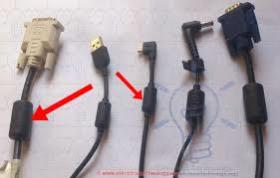 But definitely agree that if it only just fails a compliance test, and a ferrite bead worth only a few cents will fix the problem, then its a very easy decision to make. Quite a few ways to measure Vth, but for matching a series of serious switching devices, its probably the one amp to ten amp range that is mainly going to be of interest for simultaneous switching performance. A bead is not quite the same as a discrete inductor. An inductor is almost always intended as a low loss inductance that has strongly inductive characteristics. A ferrite bead is a deliberately introduced LOSSY series impedance that acts like a very small inductor shunted by a resistor. The actual added series impedance varies with frequency and works best over a certain range of frequencies that are strongly influenced by the grade of ferrite and the physical dimensions of the bead. 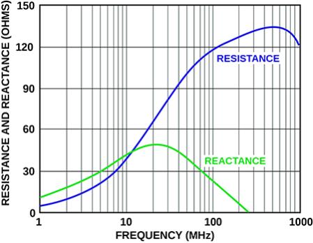 http://learnemc.com/qotw-190121 Its also interesting that adding some extra deliberate series impedance only works well in a low impedance circuit. Now we can argue all day about a mosfet gate that takes several amps to switch, but is essentially a complete open circuit under dc conditions. Is that a low impedance circuit or a high impedance circuit ? I am sure a crooked silver tongued lawyer could argue the case strongly either way. If its ringing at 5Mhz, it would require a very different ferrite bead to soak up the energy than if its ringing at 200 Mhz. So you go by the EMC test. If something nasty is happening and radiating badly at a specific frequency, you test a number of different beads to find the optimum one to soak up as much energy at the problem ringing frequency. Its still a last resort band aid solution though. Cheers, �Tony. |
||||
| wiseguy Guru Joined: 21/06/2018 Location: AustraliaPosts: 1267 |
Ahh back in the 70's my first calculator was larger than a large full size PC case and used nixie tubes a simple calculation had numbers flickering for 15 seconds lol. It used a core memory and a heap of scrs and discrete logic - what was TTL ? A flip flop took up about 4 sq inches and an OA91 straight out of the Mullard Miniwatt books cost $1.90 yep those were the days.... haha. I used Ferrite beads to solve a nasty paralleled FET oscillation issue back in 2004. Since then I always designed in a ferrite SMD part usually 1uH for FETs in parallel. Although I fully intended to use beads to solve oscillation problems I cant really predict yet what the final solution will be for my power board. If at first you dont succeed, I suggest you avoid sky diving.... Cheers Mike |
||||
| Warpspeed Guru Joined: 09/08/2007 Location: AustraliaPosts: 4406 |
Agreed, beads are excellent for making the circuit lossy at radio frequencies, and would work well at solving oscillation problems. I have never experienced oscillation problems myself, and I cannot recall anyone here on the Forum having that problem either with their inverters. But its always good to have a few more tricks and solutions available than needed to get something working. Cheers, �Tony. |
||||
| wiseguy Guru Joined: 21/06/2018 Location: AustraliaPosts: 1267 |
FYI here is a poor screen shot of the gate drive of 2 paralleled FETs from Advanced Power Technology that caused us lots of grief in 2004. They worked fine when we paralleled 2 x APT20M45BVR and oscillated like crazy with with APT20M36BLL's at around 83mHz. 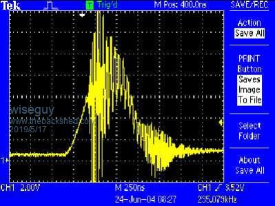 No combination of snubbing increasing/reducing gate drive resistors local bypassing etc worked, but after being instructed by engineers at APT to put a ferrite bead on the gate drive resistor leg, sure enough this cured the issue totally. I went to my junk box and found an old modified and unmodified FET module PCB. You can see the FETs each have a separate bead & resistor added, The original PCB just tied the gates together which was fine with the original FETs. This second photograph shows similar mounting of the FETs I intend to use for my inverter approach. If at first you dont succeed, I suggest you avoid sky diving.... Cheers Mike |
||||
| BenandAmber Guru Joined: 16/02/2019 Location: United StatesPosts: 961 |
Hello everybody I figured out where all the big boys hang out And warpspeed I would have love to be part of That 70s me and my wife both was born in the wrong generation Is around 130 mm by 30 mm too big for a choke just rough guesstimate I was reading poida the greats post a few pages back and got a little bit concerned I have a smaller one already to go if so Thanks for your time be warned i am good parrot but Dumber than a box of rocks |
||||
| poida Guru Joined: 02/02/2017 Location: AustraliaPosts: 1464 |
Part 33: Understanding the different PWM modulation schemes There is more than one way to skin a cat. A DC - AC inverter takes a DC supply and produces an AC output, usually using a transformer for the output, taking a high current lower voltage AC supply and converting it to the desired high voltage AC output we need. Most inverters we care about use a nominal 48V DC supply and make a nominal 240V 50Hz AC output. Most people here built a PWM inverter, and used the EG8010 IC. How you get an AC output from DC is all in the fact that there are two outputs of the inverter full bridge, and they are connected to the transformer primary winding. And, most importantly, the transformer works with the difference in the voltage between these 2 outputs. First, the two outputs of the EG8010: 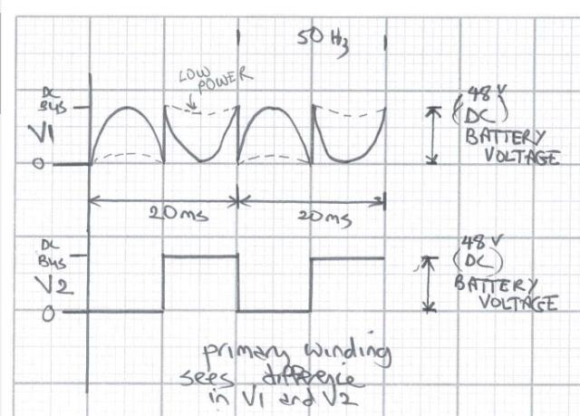 We see output "V1" is the fast PWM output, producing the sine wave approximation. V2 is the so called "fundamental" which just makes a 50Hz square wave. The transformer sees the voltage (v2-v1) which works out to be a sinewave of plus and minus the DC supply voltage. Next is my own code "2xsin", where both V1 and V2 are modulated sine waves: 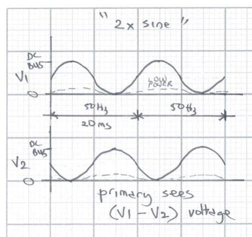 Here there is no 50 Hz square wave. In practice I found this scheme made a smoother AC 240V output waveform with far less "wiggles" This scheme results in 2x the MOSFET switching losses. Even though there are times when both V1 and V2 are the same voltage, there will be no current flow through the primary winding because they are the same voltage. This situation occurs 100 times a second with the 2xsin code. Finaly is the nanoverter output: 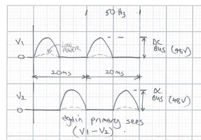 After a suggestion from Wiseguy, I produced code that made the above modulation. This again results in very smooth 240V AC voltage waveforms. It does not come with the 2x switching losses either. I think this scheme is to be preferred over the other 2. Finally here is the street power, again looking at the voltages of 2 wires, Live and Neutral. It's all the same. There will certainly be present some small voltage on Neutral, when measured to GROUND and this usually is never a problem due to household appliances and power supplies etc all running isolated offline power conversion. Nearly all current flow passes between Live and Neutral. When a little too much current passes from Neutral to GROUND or Live to GROUND, the house's RCB trips. 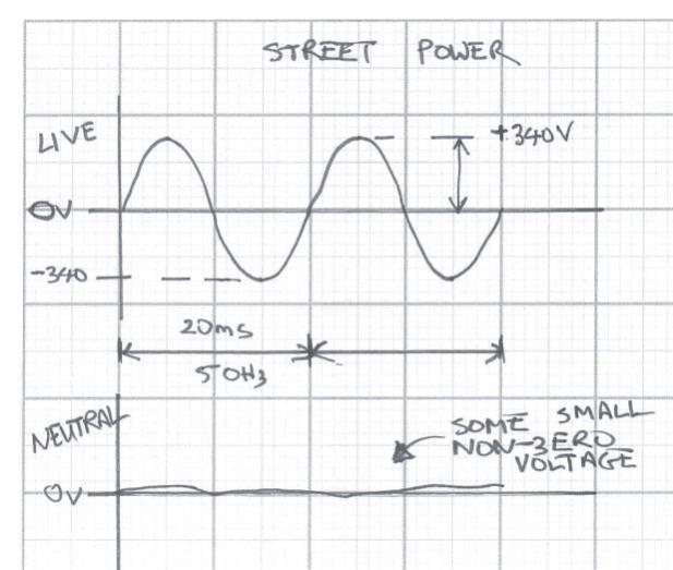 wronger than a phone book full of wrong phone numbers |
||||
| poida Guru Joined: 02/02/2017 Location: AustraliaPosts: 1464 |
Part 34: More tests with ferrite beads Earlier I showed how a ferrite bead (of some inductance value, chosen at random!) could profoundly effect the low side gate voltages, and the oscillations of the low side switch. There remained some oscillation on the high side switch. I wondered if a bead on the high side Source would help. Here are the DSO captures of the same switch events, when I placed a similar ferrite bead on the high side MOSFET Source pin, as well a bead on the low side Drain pin. Light Blue is low side gate voltage, Dark Blue is high side gate voltage. Same test conditions as the previous test.  This does not look good, look at the high side dip. Looking closer we can see it is now a poor switch transition.  Here is the event around 8.7ms, the same as that where there was a lot of HF oscillation in the previous test.  Just one ferrite bead, on the high side Source pin does this? Close-ups: 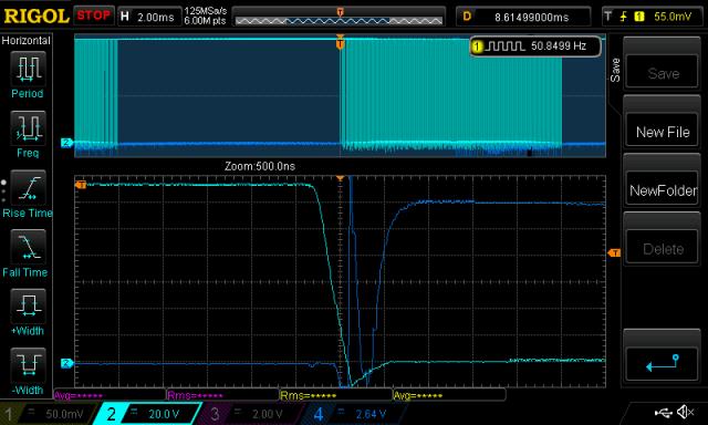 and 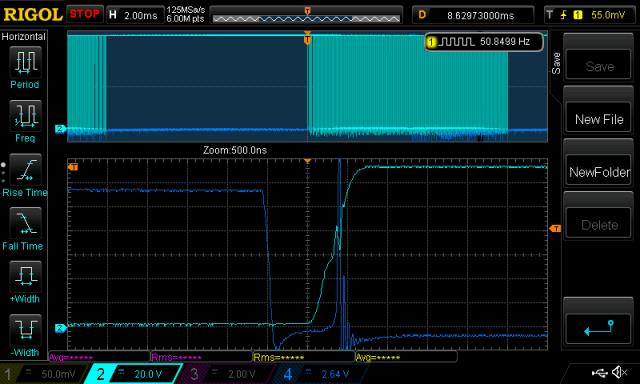 The inverter did not complain at all with this poor gate control. And the idle DC current stayed at about 0.4A, which is nominal. So, this bead had to go, it takes me 10 minutes to change it to the high side Drain. This is what I see with beads on both low side Drain and high side Drain: @1.3ms into the 1/2 wave  5ms  and 8.7ms 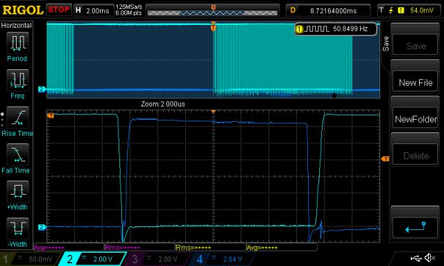 Much better, and improved over no beads on either MOSFETS. Comparing the current situation (bead on low side drain and high side drain) at 500ns/div we see little oscillation and smooth transitions. 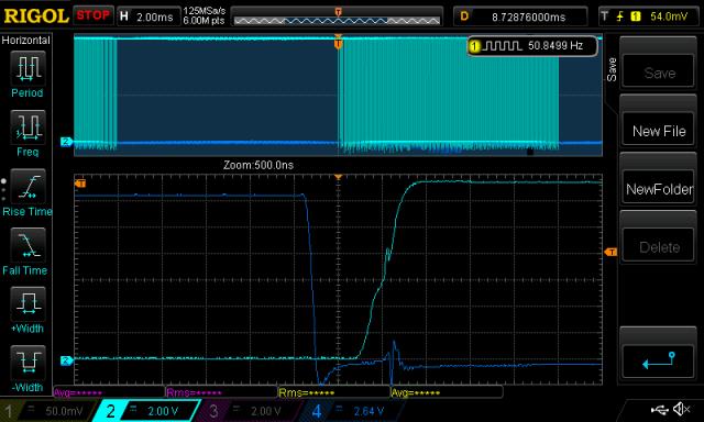 ..with only a bead on the low side drain 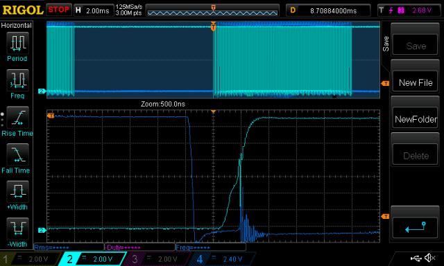 Night and day. So I like ferrite beads on the Drains (middle pin) of both the low and high side MOSFETS because those I used in this test reduced to a large degree high frequency oscillations of the gate voltages. These large changes in gate voltages are causing large current switching, at high frequencies to occur, heating up the MOSFETs unnecessarily and potentially damaging the gate's oxide layer, shortening it's useful life. And wasting a bit more DC supply energy. I might place some ferrite beads on the gates of the MOSFETS, but not these large value beads I have. I need to get some small value items and do this test again. wronger than a phone book full of wrong phone numbers |
||||
| BenandAmber Guru Joined: 16/02/2019 Location: United StatesPosts: 961 |
I have a question for everyone is there a cad file for a main board that works good with the Nano control board I could send off and have my own mosfet board made because the shipping seems to be pretty expensive from Australia to the United States The inverter that poida the Great designed for me ( really appreciate it) Has a Transformer that is skinny and tall made up of four small transformer cores It is about 1 volt per turn the idle current of the inverter is .29 and it has a large case fan that runs constantly The idol current seems to be a lot lower than the other Transformers that I have that are factory made in normal shape This is my assumption with my very little knowledge but this does seem to be true to me Have I stumbled upon something here (Forrest Gump Style) or am I just imagining things be warned i am good parrot but Dumber than a box of rocks |
||||
| azhaque Senior Member Joined: 21/02/2017 Location: PakistanPosts: 131 |
Hi Ben&Amber The main board and the transformer aren't related. You could use an E-I type of transformer with the main board, like I am using. Your transformer is tall and skinny because of difficulty in finding an appropriate core to handle 10,000 Watts. So you had to stack up 3 or 4 cores to get to your 10000 watts. In doing that you created the transformer with the Twiggy looks. So its really the difficulty in getting cores that is the issue and not the main Board. I may suggest that a potential path to pursue for you is to get a second hand slitting machine and buy CRGO sheet and slit away cores of various power levels ( 2000 Watts, 5000 watts 10000 watts etc.) and sell these on ebay. Once that part is organized then start manufacturing the main board too. azhaque |
||||
| BenandAmber Guru Joined: 16/02/2019 Location: United StatesPosts: 961 |
The Transformer with the 4 cores is for the little 4 mosfet China board inverter What I'm trying to say here is the idle current is very low when running it Seems a lot lower compared to other Transformers So is a tall skinny Transformer better in some way then a short fat one Or is my ignorance showing here in some way be warned i am good parrot but Dumber than a box of rocks |
||||
| arthur8 Regular Member Joined: 08/05/2019 Location: BrazilPosts: 69 |
Excelent topic. Will be reading it entirely before making my own ozinverter. |
||||
| wiseguy Guru Joined: 21/06/2018 Location: AustraliaPosts: 1267 |
Poida, the final 2 pictures on your recent post may have important detail that should not be overlooked. The very bottom picture shows a steep dip around the miller plateau voltage area. It appears to me that there is excessive impedance in the gate drive and it is not "stiff" enough. It gives the appearance that the gate resistor might be too high or the gate drive current is too low. I have seen that FETs can have a tendency to oscillate if they travel too slowly through the miller region. I am unsure of the gate resistors or buffer being used but each FET should have at least 2A to 2.5A drive current in my opinion, that would have them switching in ~ 100nSecs. If you are using 10 Ohm resistors and combine this with the FETs 3 Ohms gate resistance the max current from 13V gate drive would be 1A. 1 Coulomb is 1A.Second. The gate charge is of the order of 200nC so we would require 1A for 200nSec to turn on. (these are approximate values but should be well in the ballpark) Then there is the Cgd (~75nC) that injects opposite polarity charge to the gate drive and slows down the drive further, the higher the drain voltage being switched the greater the (bad) effect Cgd has on the drive signal. I believe it is this effect that is visible in the last picture trying to turn off the gate drive as the drain voltage rapidly falls as the FET turns on. If the gate resistance is lowered by half or more to increase the gate drive, that dip in the miller plateau region might go away. I see and agree that adding the ferrite beads appears to minimise the dip (it is just still visible) perhaps adding the ferrite beads slows down the rate of change on the drain enough, reducing Cgd effects. If we add parts it is good to know that we are doing it for the right reasons and perhaps not masking another underlying issue that may still be borderline. I am a big believer in belts and braces - if there is not enough gate drive increase it and if still required perhaps also add the bead for good measure. The beads sure helped me with the oscillations I had on the Drain of my FETs but my gate drive did not display those negative dips in the miller region. I used 10 ohm gate resistors but I also used the IRFP4710 FETs and their gate charge is around half the HY4008 and the buffers in my layout were very close to the FETs so it is not a direct comparison. My parts have finally started to arrive so hopefully in a few more weeks I can use my own test rig for investigating these things. If at first you dont succeed, I suggest you avoid sky diving.... Cheers Mike |
||||
| poida Guru Joined: 02/02/2017 Location: AustraliaPosts: 1464 |
Part of my aim is to look at the inverter and see what things could be done to improve it, without redesign. Other aims are to help bring to light design concepts that we would need to employ for a reasonable return on effort and cost. I am in the "hacking existing design mode" with the Madness power board. It uses the TIP41/TIP42 totem pole drive, with a 10R gate resistor, and a 10KR on the gate to Source. (Is this correct Madness?) I can probe the voltage across the 10R resistor, which will give us current. And with a little work, integrated over time, this will be charge. Time I have a look at switching times and currents for the HY4008? wronger than a phone book full of wrong phone numbers |
||||
mackoffgrid Guru Joined: 13/03/2017 Location: AustraliaPosts: 460 |
Mike, my view that this is not particularly a drive problem. The oscillation appears to happen after the miller plateau, I expect Vds to have started moving by this point (probably finished ) and what we're seeing is the large change in Vds and the resultant currents forced through Cgd. A Vds trace might show this. I'm happy to be wrong - just throwing my 2 bobs worth in  Cheers Andrew |
||||
Madness Guru Joined: 08/10/2011 Location: AustraliaPosts: 2498 |
Yes 10R Gate but 5k1 and 104 cap gate to source. Been running like that 24/7/365 for over 1 year now. There are only 10 types of people in the world: those who understand binary, and those who don't. |
||||
| johnmc Senior Member Joined: 21/01/2011 Location: AustraliaPosts: 282 |
Good day The Madness 2018 power PCB I have, has 10R for the gate 20K for the gate to source and no 104 cap. Is there multiple types of Madness power boards? cheers john johnmc |
||||
| The Back Shed's forum code is written, and hosted, in Australia. | © JAQ Software 2026 |