
|

|
Forum Index : Electronics : 150V 45A MPPT - roll your own
| Author | Message | ||||
| wiseguy Guru Joined: 21/06/2018 Location: AustraliaPosts: 1267 |
Very witty comment Ryan - I appreciated it   If at first you dont succeed, I suggest you avoid sky diving.... Cheers Mike |
||||
| poida Guru Joined: 02/02/2017 Location: AustraliaPosts: 1464 |
Just tying up one loose end here. I have both Nicks power boards and one of Wiseguy's power boards. I was wondering how they compare in one aspect only, which is the high current inductive loop of the switch and DC supply caps. Wiseguy chose very well some RC snubbers to be built into his board. These are the 1nF cap and 10R resistors. There is one connecting the switch node to ground and one connecting to DC supply. The switch node oscillates quite strongly when switched ON, sending current through the inductor. The RC snubbers are used to reduce this oscillation. I have seen the amplitude of oscillation to be a large fraction of the DC supply voltage, e.g. with 110V supply, there are peaks in the oscillation that will be 150V or even more. Here is what it looks like with no snubbers, using Nick's board. This is with 57V input and 38A output and 1470W load. Both boards use the same MOSFETS and HY5110 as diodes. 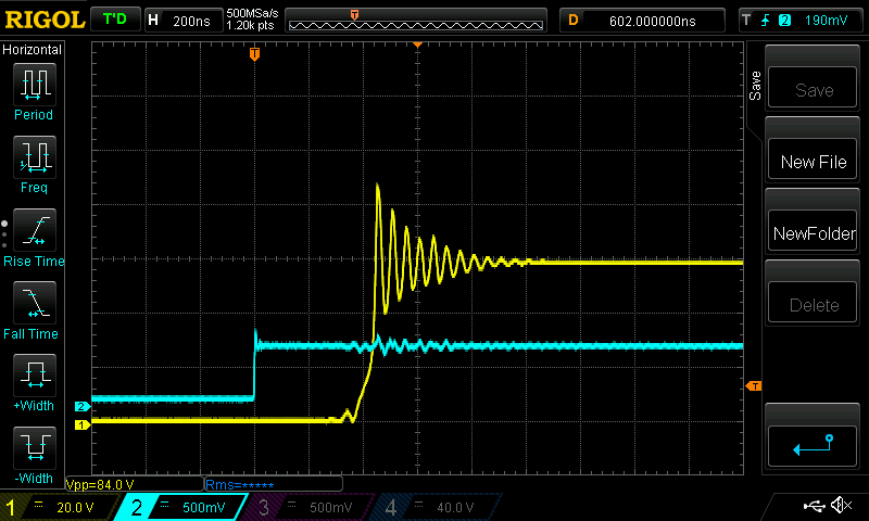 Now this is a very textbook example of damped oscillation. The frequency of this is about 18 Mhz. Here it is with a 1nF and 10R RC snubber connecting the switch output to ground and another snubber connecting it to DC supply. 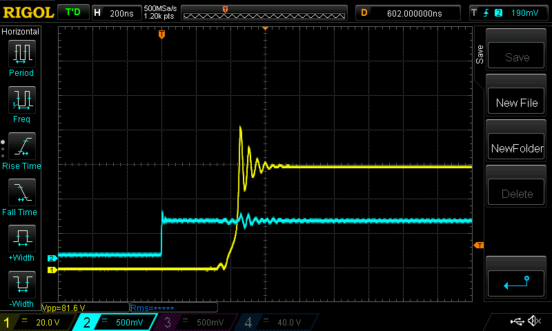 much less oscillation. great. I could not detect any increased DC supply current when the snubbers were fitted. Now, when I built Wiseguy's board, I put in place the two 1nF/10R snubbers. I can not show this board without them so here it is with them. Same DC input and load 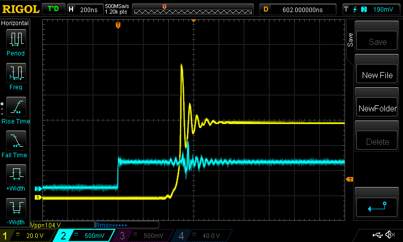 I was wondering how the HY5110 MOSFETs used as diodes would go with these sometimes 150V peaks they see. I have tested the avalanche breakdown voltage of these parts and they start to conduct strongly at about 117V and above. I think during these peak voltages of the oscillation the HY5110 conduct the switch output to ground...that is short the DC input, through the MOSFETS, through the HY5110 then to ground. Not good for efficiency for a start and probably not good for longevity either. so here is a series showing the switch node as I increase DC supply, gradually ensuring the HY5110 have higher and higher voltages to withstand. 57V input, 1730W, 39A ouput 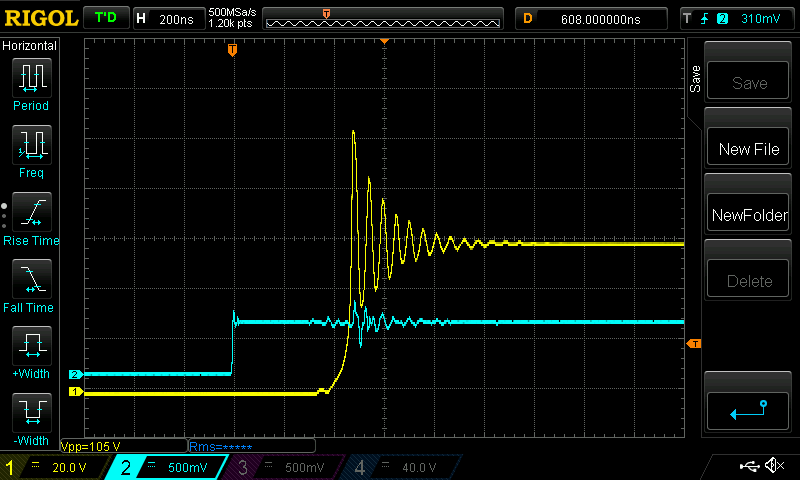 85V input 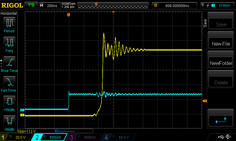 94V input clearly the high peaks are clipped and the action of clipping makes for a diode reverse recovery sort of behaviour. 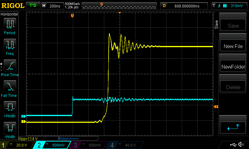 105.5V input 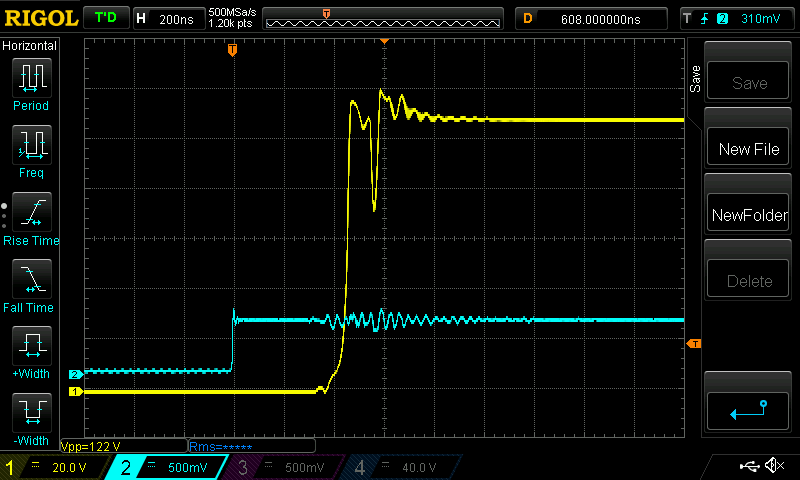 I think we need higher voltage diodes. The HY5110 are clearly exposed to too high voltages for short periods of time and so they go into avalanche mode (i.e. short circuit) and take a little time to come out of it. They permit about 115V to pass through them reverse biased but no more. The mppt works well, that is for sure. But I don't want to see us build boards that "worked well enough for Poida but mine seem to blow up too often" What to do... Get some TO-247 package switch mode supply diodes with more than 150V and 30A rating. I assume there will be 2 diodes in each package so there will be 4 diodes conducting 45A. That is about right to my mind. And not use the HY5110 MOSFETs as diodes. Maybe the MBR120150WT (60A, 150V) would be a good start point. STPS60SM200CW are 200V 60A, and $5 each. This sort of thing. Edited 2020-08-21 21:31 by poida wronger than a phone book full of wrong phone numbers |
||||
| wiseguy Guru Joined: 21/06/2018 Location: AustraliaPosts: 1267 |
Peter, what is the blue trace - is it the drive to the opto? Is the yellow trace on the Drain of the two upper switching mosfets ? This looks very reminiscent of my post "what is the ferrite bead for". The oscillations I was looking at were ~21MHz. A ferrite bead on the drains stopped it in its tracks. I know you got some results that implied the source was the best place for them, but I cant agree that the source having extra inductance is a good thing. The first thing I will do if I have these issues will be to place a bead on the drain on each of the upper mosfets. If there is still an issue I will then look at a bead on the gate. I also concur with your thoughts on using a diode instead of a lower FET. If trying to use a FET for the lower diode I would not be placing any inductance between the gate and the source (no bead on the source) I would want the gate either tied to the source as tightly as possible or even better have it biased with reverse bias. You will have more chance to try the bead reposition before me - I hope you get the results I expect. (and that you would hope for) If at first you dont succeed, I suggest you avoid sky diving.... Cheers Mike |
||||
| nickskethisniks Guru Joined: 17/10/2017 Location: BelgiumPosts: 472 |
SYM-1, it�s nice to see other people are creative and �amusing� there self�s too, that picture of your design created a smile on my face, thank you! I take my hat off for you. This is some serious overkill, I like it. But what you need to know, maybe you already know is that, that bigger is not always better. Inductance is created by distance and it will not only lower by using thicker conductors. They use laminated bussbars in high power applications to keep inductance as small as possible. Two conductors parallel (semi isolated) would half the inductance� I would add some polypropylene capacitors to your system to compensate the higher esl your capacitors probably have. Big capacitors are not really suitable for higher frequency applications. In the beginning I had some ideas for those 227 devices for 1 serious killer, but after following SolarMike's his topics I eventually decided to use several smaller controllers. And split up my solar system in 4-5 strings to spread the load and shading. I currently have 1 controller with 5600Wp panels on it, with only 2 IRFP4110 mosfets, and they see sometimes periods of more then 100Amps ( that is around 85% duty cycle for extended time. 45-50A is the continuous limit for sure per TO247 device. I made a 3 ph bldc controller with HY4008 mosfets, and current limit is set at 80A! Didn�t blow them, yet. But that is not a continuous rating and only at 50% dutycycle maximum under load. But standstill is serious and more then a few seconds. Poida So it seems the peak is less with my boards? Are the gate drive (resistors and caps) and the buffer capacitors the same? It would be nice to see if you monitor the "bus" voltage (on the drain). I suppose the yellow trace is the measured GND-Source? I think there are some things that could be improved in the design but nothing we can do about it now. The design was made with compromises, 1 of it was time and simplicity. But I think it�s a good reliable and robust design ones all parts are �fine-tuned�. I did spent time to put all �power parts� as close together as possible. Maybe some things to think about next time: (about the gate drive) -Avoiding gate traces close to power planes/traces -Gate traces as short as possible -If gate drive can�t be placed close by, using external gate driver pcb 90� on power pcb. -Or If that is not possible using external gate driver with twisted wires to the mosfets -If the gate driver traces are above the power planes, they need to cross them under 90�. -Individual turn on and turn off resistor These are all things I read about, not all things were tested by myself. What you can try to do is using higher resistance in the gate drive, that way we will probably have higher switching losses but nothing to worry about I think. But it should lower the peaks. Difference between TH and smd resistors? Making the bus voltage as stiff as possible by using low esr capacitors + polypropylene caps. I�m currently adapting(trying) Poida�s code so I can monitor and adjust some parameters over RS-485 or rs-422. I wanted the controller to act as a �slave� with a unique ID number, that way many slaves can be connected to one bus and will only talk to the master. I think I got it close now but I can�t guarantee the code is working like it was meant, yet. I didn�t understand much about rs-485 and so I was hoping if I used full duplex I could just convert the uart to rs-485 without pulling pins high or low. Guess what, that didn�t work well� So I had to use an extra output pin to pull DE pin(I�m using sn65175) up only when that slave wanted to sent data. All other slave connections (the transmitters) had to be disabled. The code is working for full duplex (rs-422?) but I suppose the code should work for half duplex Rs-485 as well. I will post the code ones it is fully working. The aim is to do the same for the Nanoverter, but first I need to write some code for the master, RPI with Nodered for the GUI. Anyone that could advise me about some rs-485 drivers suitable for 3,3V and 5V, I want to use them for my bms and other systems as well. |
||||
| Warpspeed Guru Joined: 09/08/2007 Location: AustraliaPosts: 4406 |
I think there comes a point where it all becomes increasingly difficult to build a very high powered buck regulator all in one single lump. It all becomes so much easier to design something for say twenty or twenty five amps using a single mosfet and a single diode, and reasonably sized heatsink and inductor, and some suitable low esr electrolytics. All the lead lengths can be kept very short where it really matters, and the layout fairly simple and direct. Then simply parallel up as many of the above individual power modules as may be required. No problem with driving them all together in phase from a single software "brain". As far as I know, its never been tried, but a similar approach to building a very high powered PWM inverter might prove less troublesome than trying to parallel up more than two mosfets in each leg of a PWM bridge. Each module could have its own choke feeding a common 50Hz step up transformer. The advantages would be that it would current share much better between mosfets, and the dynamic switching times of individual mosfets would no longer be so critical. I have no personal interest in pursuing any of that myself, since my Warpverter solves all of the problems associated with high frequency PWM at high power levels. Building a monster single stage buck converter has many of the same issues as building a high powered PWM inverter. Its definitely not as easy as it at first appears. Edited 2020-08-22 08:08 by Warpspeed Cheers, �Tony. |
||||
| wiseguy Guru Joined: 21/06/2018 Location: AustraliaPosts: 1267 |
Whoops, that is supposed to say; Is the yellow trace on the Source of the two upper switching mosfets ? and I got more wrong - note to self "stop posting when tired' The first thing I will do if I have these issues will be to place a bead on the drain on each of the lower mosfets(diodes) but do first remove the Source fet/diode bead if it is present for the lower fet/diode. If there is still an issue I would then look at a bead on Drain & then on the Gate of the upper mosfets. I agree with Warp to a point, it is a bit of a black art & As Nicks said previously that electronic issues always have a reason - you just need to find it ! I am confident that we can end up with a working high powered buck without it being a pulsed 20MHz transmitter - you just need to find that whoa camel moment ! Although the lower Fets are "OFF" at the oscillation point I believe they are/may be the real culprit. Lastly these oscillations do not need to be due to passing very high currents and can actually occur when passing next to zero current - they just dont go away at higher currents. Edited 2020-08-22 08:49 by wiseguy If at first you dont succeed, I suggest you avoid sky diving.... Cheers Mike |
||||
| wiseguy Guru Joined: 21/06/2018 Location: AustraliaPosts: 1267 |
I would like to know where this limit of 45-50A for a T0247 has its origins ? �Please refer me to a reputable source. My past experience, the information on the data sheets and my calculations dont seem to support this. Manufacturers data sheets eem to implly Quote " Current limit #1 defines the area limited by the drain current rating. For continuous-current (DC) operation, the SOA is constrained by IDmax. For pulsed operation, the SOA is bound by the IDPmax line. I have never seen a secondary note that the SOA limits are superseded/reduced with a current limit for the connection legs. Edited 2020-08-22 09:20 by wiseguy If at first you dont succeed, I suggest you avoid sky diving.... Cheers Mike |
||||
renewableMark Guru Joined: 09/12/2017 Location: AustraliaPosts: 1678 |
OK so there is one bead for the connection on the board (close to c17), and also for the fets. What beads are being used? Or shall I wait for your further tests? The only ones I have are this type Edited 2020-08-22 09:19 by renewableMark Cheers Caveman Mark Off grid eastern Melb |
||||
| wiseguy Guru Joined: 21/06/2018 Location: AustraliaPosts: 1267 |
Mark - I think you should delay installing the Power Fets / diodes until this is sorted. I think I need to find the time to build my power board as fast as I can - its not fair to dump everything on Peter to solve. Desoldering big leads from a 2 0z board with no thermal reliefs can be challenging to not cause damage. If at first you dont succeed, I suggest you avoid sky diving.... Cheers Mike |
||||
| poida Guru Joined: 02/02/2017 Location: AustraliaPosts: 1464 |
yes, Blue is drive to Opto. Yellow is as shown below. 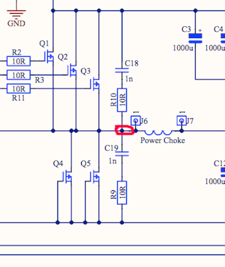 I call that location the switch node. Nearly any other location is either DC input or DC output or ground. As soon as I get the wood heater powered up I will do this. 5 deg C outside and rain. I do recall the beads on the Drain tests you did. Time to see how they go on the powerboards. Edited 2020-08-22 09:40 by poida wronger than a phone book full of wrong phone numbers |
||||
| SYM-1 Regular Member Joined: 18/10/2019 Location: New ZealandPosts: 45 |
My sources were not referenced to any research but we can look at some fundamentals like the power we need to dissipate at a given lead size and current. What are the reasons for avoiding high currents in small leads? Efficiency and temperature rise. Even at 100 Amps the efficiency loss is not terribly high compared with the loss in the FET so temperature remains the issue. What is the issue with temperature rise? I guess my greatest concern is heat flowing back into the FET junction and causing failure of the FET due to over temperature. What temperature rise you get with a given power dissipation depends on how you get rid of the heat. For instance bolstering the thickness of the leads may help. Ultimately I think it would be a useful experiment to measure the temperature at various currents. A low thermal inertia probe would be necessary but I think I can find one of those amongst my spares. What I would propose is to drive the FET continuously with a low resistance load till the temperature rose to 70 degrees or a temperature equilibrium below this. This would be controlled and measured by a brain board of some sort. Persistence is the key |
||||
| poida Guru Joined: 02/02/2017 Location: AustraliaPosts: 1464 |
.. Poida So it seems the peak is less with my boards? Are the gate drive (resistors and caps) and the buffer capacitors the same? It would be nice to see if you monitor the "bus" voltage (on the drain). I suppose the yellow trace is the measured GND-Source? .. I believe both boards are using very similar buffer caps, the same 10R gate drive resistors, the same opto drive IC. The yellow trace is the switch node (output to the inductor if you like) with ground connected to the ground plane taken off a pin of one of the diodes. I think the DC Bus voltage will be quite stable and all I will see with my inferior probe technique will be EMI on top of the bus voltage. I can do that today. wronger than a phone book full of wrong phone numbers |
||||
| wiseguy Guru Joined: 21/06/2018 Location: AustraliaPosts: 1267 |
Sym1 my comment on asking for a reference source for the 45-50A was not aimed at you. After you said that, I showed with a calculation that 2cm of the thin leads was only around 10% of the channel resistance and the channel is just a bit of conducting sand but rated at 150A so the legs should not vaporise any time soon. (And the conducted heat back into the FET should only contribute maybe 5-10% of the total generated heat). It was the reinforcement comment made by Nicks that "for sure 45-50A is the limit". �That is when I asked for a reference where this comes from. The nearest reference I could find was around 75A for a flimsier TO220 lead. If there is information or knowledge available - I would love to learn or be educated by it but I don't go much on hearsay or gut feeling - unless or course its my gut feeling lol. Edited 2020-08-22 11:35 by wiseguy If at first you dont succeed, I suggest you avoid sky diving.... Cheers Mike |
||||
| nickskethisniks Guru Joined: 17/10/2017 Location: BelgiumPosts: 472 |
It was late when I was writing too.  �I know there is more to it then just say, hey that mosfet can switch 50A. �I know there is more to it then just say, hey that mosfet can switch 50A. I�m not going to argue with the fact they can deliver more then 75A, I know that they can, the wires running to my 3ph motor are running hotter then my mosfets in the controller. I can�t prove or document my 50A statement, but I use that as a good number to start with when designing something new. I never was a professional E designer and never will be, it�s only the last 5 years I�m gaining good experience in power electronics. And the learning curve is endless. But one thing I learned was that we need to put everything in the right perspective. So in this case it�s maybe better to start talking in another perspective, we probably need to discuss the amount of power dissipation they can handle. Because there are a lot of TO247 mosfets that can�t even handle 50A. The circumstance matter a lot it�s not the mosfet that is the limiting factor in most cases, you have the pcb where the traces are not big enough to carry those big currents and also the heat generation, you will start creating big temperature differences and on the long term you will get metal fatigue with bad solder joints to give just one example. I know that you know all that Wiseguy and you made a fair point questioning my statement with reason. In my solar controller it�s not safe to push the mosfets beyond 50A because the tracks on my pcb�s get to hot, and the mosfets are placed to close to each other to efficiently remove all the heat on that spot off the heatsink. I still remember you and warpspeed gave suggestions how to improve the heattransfer between the heatsink and mosfets. For example I forgot who it was but someone on this forum tested his HY4008 mosfets to a point of failure, he found they were reliable for using them to 2000W in a 4 mosfet H bridge. But his findings were based under certain circumstances. What I did find (I�m following a guy on endless sphere, Zombiess, spending a great amount of time testing and doing research in this matter. So I looked up a post of him doing some temperature testing of IRFP4668 mosfets. He did some testing of those mosfets on a active cooled cpu heatsink. He set 70�C as the maximum safe case temperature of the mosfet, above 80�C he experienced thermal runaway will happen very quickly. � He tested different isolation options, that is the most limiting factor. But also his findings were based on certain constraints., active cooling, certain ambient temperature,... I could give a resume but there would be information lost I guess. It's better you (all) read the post yourself, if you have time you can find it here: (somewhere in around post 10) Link To be back on topic, I still haven�t received all of my higher voltage parts� So can�t do testing at the moment. Edited 2020-08-22 19:57 by nickskethisniks |
||||
| poida Guru Joined: 02/02/2017 Location: AustraliaPosts: 1464 |
Ok, here is a big post. First, this is the test power board. I don't want to keep hacking at the one and only Mike's board or the good Nicks board which I plan to replace the $1,000 Morningstar mppt with. It also is a test bed for wrong capacitor choices. Only 4 x 470uf on the input and one 10,000uF on the output. I wanted to see if my firmware would be upset by this. (tests have shown there is no problems) here is the board with the two test points (the switch node and the DC bus voltage) 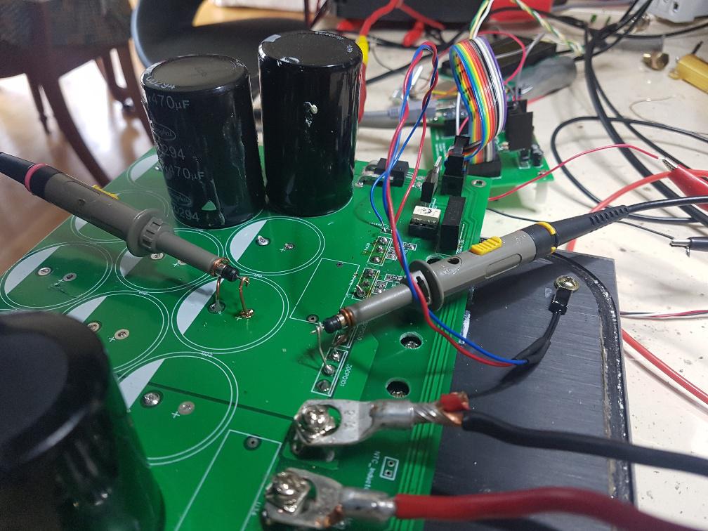 and here are the results of various experiments and MOSFET change overs. pretty ugly eh? 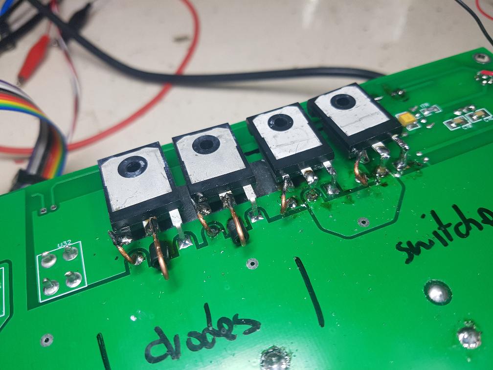 Yellow is switch node, Purple is DC bus voltage, Light Blue is opto drive input. 105V input, 1500W out,40V Here are no ferrite beads on any pins. 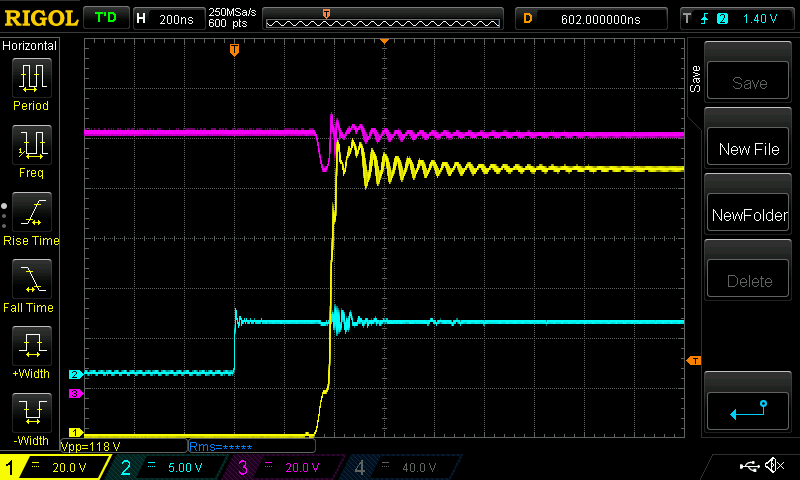 this is so much better. I ask myself "why did I use beads anyway?..dickhead" No nasty dip in the switch node voltage as the diode conducts due to over voltage for the device. Here it is with the 1nF/10R snubbers 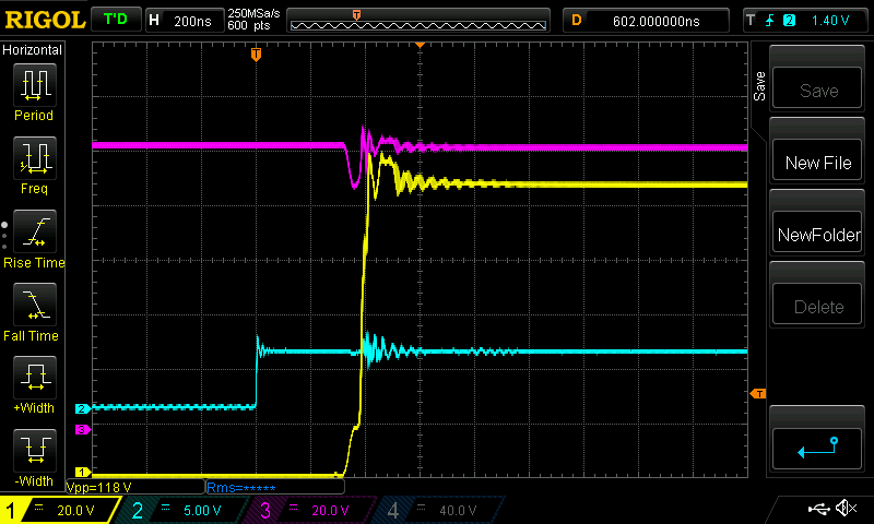 Less of that high frequency ripple, which was not a problem to me anyway. The 1/4W 10R resistor gets far too hot, I would use a 1W in this case. Wiseguy, thanks for pushing me in certain directions. I doubt I would get there by myself. No more high voltage oscillation, no more shoot through. No more likely damaging high voltage & high current spikes commuted by the diodes. Here is Wiseguy's board with the beads removed. I built it with 2 MOSFETS and 2 HY5110 as diodes. The switch ON event.. 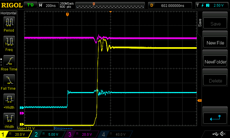 No evidence of shoot through, no significant oscillation. Just really nice. And the switch OFF event. Just about as perfect as you could get. 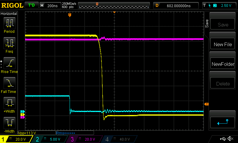 So again I find myself chasing phantoms. In this case I chose to use ferrite beads on certain pins. And saw the results and thought something is wrong. And did not think it was the beads that were the problem. But experiment after experiment lead me to a better place. Eventually. From what I see in the last two DSO images, I think the design is proven to be good to go for input voltages up to about 105V. I will be testing 200V "real" diodes in the coming weeks, and that should allow the design to get up to 150V input. wronger than a phone book full of wrong phone numbers |
||||
| poida Guru Joined: 02/02/2017 Location: AustraliaPosts: 1464 |
And for Nicks, here is his board, tested under identical conditions. Same input voltage, inductor, but a bit more output power, 1800W. First with the beads. Which cause problems. one being the deep dip in the switch node voltage just before the center line. This is due to the diodes having their reverse bias voltage exceeded and so they conduct. Not good at all. 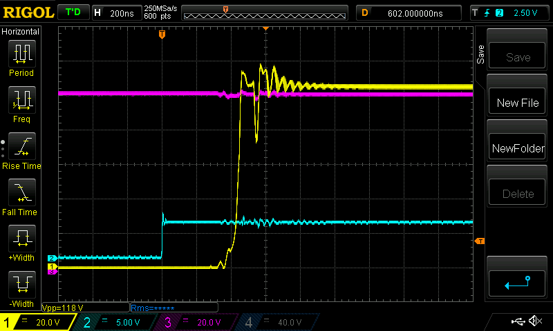 Now with the beads removed. 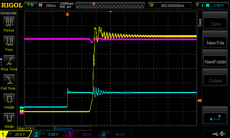 Much nicer. And with the two snubbers. 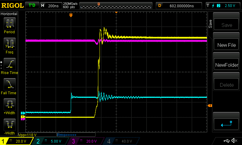 and finally the switch OFF event, with snubbers. This is the same as without snubbers. 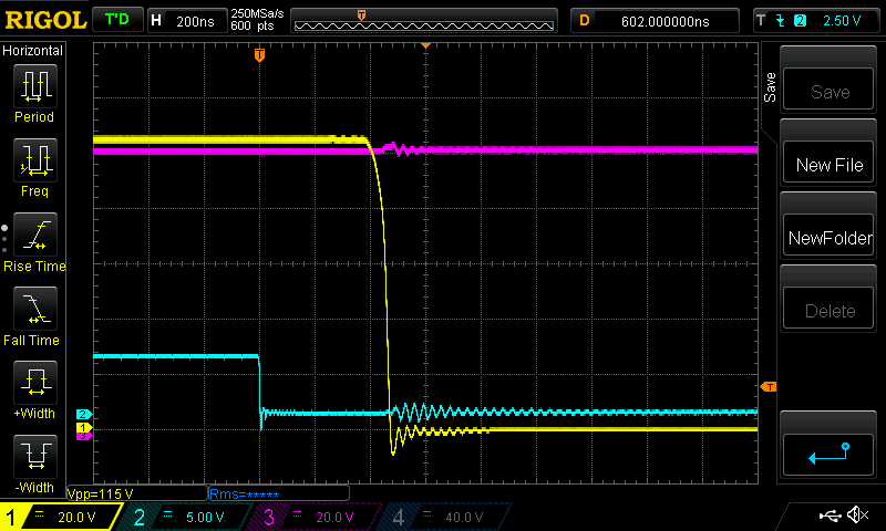 I think I am operating at the maximum voltage for the HY5110 body diodes. Even backing off 10 volts will be enough to prevent any issues of over volting the diodes. The 1/4W 10R resisitor gets so hot it discolours in 2 minutes. I suppose some effort in choosing RC snubber values might be worthwhile. These tests show Nicks' boards work well too. wronger than a phone book full of wrong phone numbers |
||||
| wiseguy Guru Joined: 21/06/2018 Location: AustraliaPosts: 1267 |
The 1n & 10R were not calculated - it was just meant as a starting point and a number to hang on the parts & to remind me to allow for them. A real diode in the lower leg may benefit more with the snubber than the FET, time will tell. I believe the dip in the supply was caused by slight commutation of the lower FET. I am not convinced that we can't end up with a cleaner waveform than the two/few cycles of oscillation we still see when the choke node is first driven high. But I volunteer to achieve that - that might also cause a bit of extra heat in the snubbers. All in all it looks a lot better than that big decayed ring we started with - it must be beer a clock time  PS I always leave the snubbers off until absolute last as they may be masking what is happening underneath. If you look at the second to last picture, the gate drive is still ringing like crazy. I am sure it is reflected oscillation from the Drain even though the snubber might be masking (swallowing) a lot of the energy so the drain looks half reasonable. I still think we might benefit from a bead somewhere ! Edited 2020-08-22 19:29 by wiseguy If at first you dont succeed, I suggest you avoid sky diving.... Cheers Mike |
||||
renewableMark Guru Joined: 09/12/2017 Location: AustraliaPosts: 1678 |
I have 5 of these if you want to test them Peter. Cheers Caveman Mark Off grid eastern Melb |
||||
| poida Guru Joined: 02/02/2017 Location: AustraliaPosts: 1464 |
Mark: I could fit 2 to a board and see the difference. Only if you can spare them. Did you buy more for your own boards? wronger than a phone book full of wrong phone numbers |
||||
renewableMark Guru Joined: 09/12/2017 Location: AustraliaPosts: 1678 |
I know how stuff often gets tweaked so I only got five. If they work fine I'll get another five and will have an even number. maybe something with a bit more headroom may be wise though 200+v? Edited 2020-08-22 20:48 by renewableMark Cheers Caveman Mark Off grid eastern Melb |
||||
| The Back Shed's forum code is written, and hosted, in Australia. | © JAQ Software 2026 |