
|

|
Forum Index : Electronics : Power Supply Upgrade.
| Author | Message | ||||
| Warpspeed Guru Joined: 09/08/2007 Location: AustraliaPosts: 4406 |
Klaus has just PM'd me asking if I have a circuit diagram for that e-bay bench power supply kit. All I have are some nasty rough pencil sketches that I traced out the hard way. As images cannot be attached to PMs, I will post them here, it may be of some assistance to others. I hope to eventually draw the circuit properly, but its on my fairly long to do list. 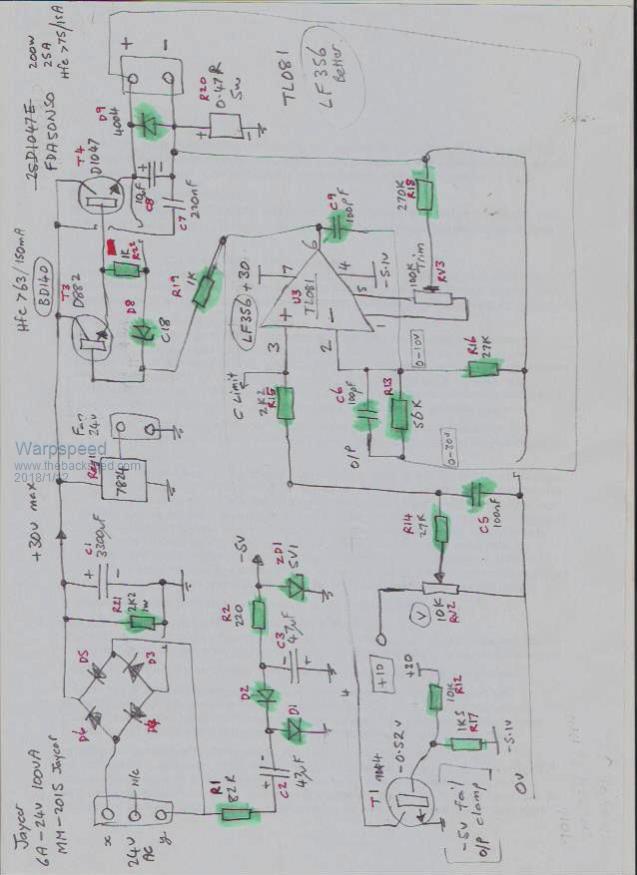 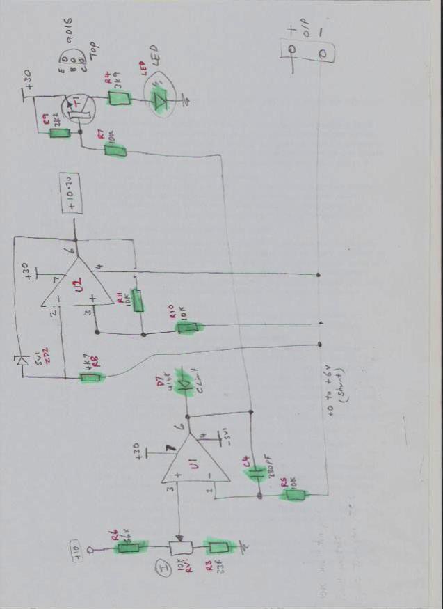 The circuit board only has component values on it, no component designators. So I had to invent my own component designators so parts on the schematic can be located on the board. 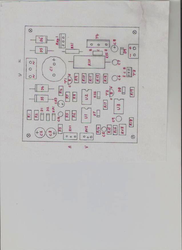 A few observations and changes that I have made to my own power supply. The rather curious circuit round T1 is to clamp the output of U3 hard to ground if either of two things happens. Its rather faint on my schematic, but the collector of T1 is tied solidly to U3 pin 6 output of the op amp. If the 5.1v negative supply fails or if the 30v incoming supply is excessive. Resistors R12 and R17 have been chosen to bias T1 off when both power rails are up and correct. If something is wrong pin 6 of U3 gets clamped to ground by T1 reducing the output from the supply to zero. If your supply appears dead when you first power it up, check that the 30v dc rail is not too high. This could cause a lot of anxiety during the initial first test if you are not expecting it. Its actually quite clever protection. Another thing I discovered, the 5.1 volt zeners that come in the kit are not very accurate. ZD1 does not matter, but ZD2 is fairly important, otherwise your 10.2v dc reference could be a long way out which can cause the potentiometer ranges to be out. You will get something other than 0-30v and 0-3A if the internal 10.2v voltage reference is too far out. A couple of extra 22pF capacitors came in each of the five kits I now have, they are not used, and were included by mistake. The 2SD1047E bipolar output transistor is running right on its safe operating area limit, even with an infinite heatsink. Throw it away and replace it with a nice beefy mosfet. Amazingly, that can be done without any other significant changes to the circuit. Hint... Don't be to concerned about voltage rating or Rds on. In linear operation, Rds on has no real meaning anyway. What you want is a real monster fet with the largest possible silicon die inside. A clue to that will be the rated power dissipation on the data sheet. The mosfet I used (simply because I had some) was an FDA50N50. Available on E-bay. These are rated at 500v and 48 Amps, ridiculous for this, but it has a very nice juicy 625 watt power rating (at an unrealistic 25C junction temperature). http://html.alldatasheet.com/html-pdf/90595/FAIRCHILD/FDA50N50/407/1/FDA50N50.html That must be de-rated of course, for actual operating junction temperature, but its still a mighty big chunk of silicon inside there, which is exactly what we are looking for. Its all about efficient heat transfer.... And that is much more important than specified voltage and current maximums for this type of application. If you short the output, with three amps set, there will be something like 90+ watts dissipated. The original D1047 supplied in the kit will not stand that for very long. If its just a "whoops" and you remove the output short on the power supply it will probably work fine. If you run three amps into a dead short with a big mosfet it will run like that continuously forever, as long as the heatsink and fan are large enough for 90 watts continuous dissipation. If you do the big mosfet trick, the original base driver T3 then has almost nothing to do, and you can leave off the small heatsink. I now have two of these supplies built and working wonderfully well, and have almost completed building three more! Just need boxes and transformers to finish these last three off, but there is no hurry. Ten turn pots are highly recommended. Altogether pretty good value and its all been pretty well thought out by someone. The original output transistor is a bit wimpy for really heavy duty idiot proof use though. I mounted my mosfet into a three way screw terminal block. It makes replacement dead simple if it ever spits the dummy. Ah! one detail I almost forgot. D8 as supplied in the kit is a diode, its purpose is to discharge any capacitance on the output so that you can adjust the output up and down without any load or a bleed resistor on the power supply output. I replaced D8 with an 18 volt zener diode. In the diode direction it performs the exact same function as the original diode. But this new zener now also protects the mosfet gate from possibly seeing the full 30 volts under some fault conditions. If the power supply output is dead shorted, this 18v zener and resistor R19 pretty much guarantee the mosfet gate can never see more than 18v. Cheers, �Tony. |
||||
| Tinker Guru Joined: 07/11/2007 Location: AustraliaPosts: 1904 |
Thanks Tony, Very comprehensive details, as is usual from you and very much appreciated by your forumites. I will incorporate your suggestions and also draw the schematic shortly. You can then check it for me. Now, I got to figure out a way to print out your message... Ah, figured it out: just do a ctrl P but one has to guess on which page the part one wants printed falls or the whole kaboodle gets printed. Klaus |
||||
| Warpspeed Guru Joined: 09/08/2007 Location: AustraliaPosts: 4406 |
Can you do a "cut and paste" for the text into a new document, and a "save image as" for the circuits. At least that is how I do it. Sorry about the crappy circuit, it was never meant to be posted in that state. But I figured you would rather have something right now rather than nothing. Pretty pleased with how these bench supplies are turning out. Cheers, �Tony. |
||||
Madness Guru Joined: 08/10/2011 Location: AustraliaPosts: 2498 |
These are only $5.75 delivered from Aliexpress There are only 10 types of people in the world: those who understand binary, and those who don't. |
||||
| Warpspeed Guru Joined: 09/08/2007 Location: AustraliaPosts: 4406 |
Like Wow ! You still need a transformer, box to put it all into, a very large heat sink, and panel meters. The final cost is probably not that much different to a fully built Chinese switched mode bench power supply. The big advantage though, when the Chinese supply blows up its not going to be repairable. It will be a surface mount board, and have tiny unidentifiable components and no circuit diagram. An assembled kit of parts using large simple readily available through hole parts is easily repairable. These kit circuit boards are very robust with broad tracks, and large pads and holes, very easy to work on. Especially if you use IC sockets. If you read all the warnings that come with those Chinese bench power supplies, they sound far too fragile to be used as a hack every day bench power supply. Cheers, �Tony. |
||||
Madness Guru Joined: 08/10/2011 Location: AustraliaPosts: 2498 |
I have an old amplifier that has the case, heatsink and big transformer with multiple taps. Also somewhere on here is some hacks on computer power supplies, they can deliver substantial current and if you blow one up there is plenty more available. There are only 10 types of people in the world: those who understand binary, and those who don't. |
||||
| Warpspeed Guru Joined: 09/08/2007 Location: AustraliaPosts: 4406 |
Have two going and most parts to build three more. 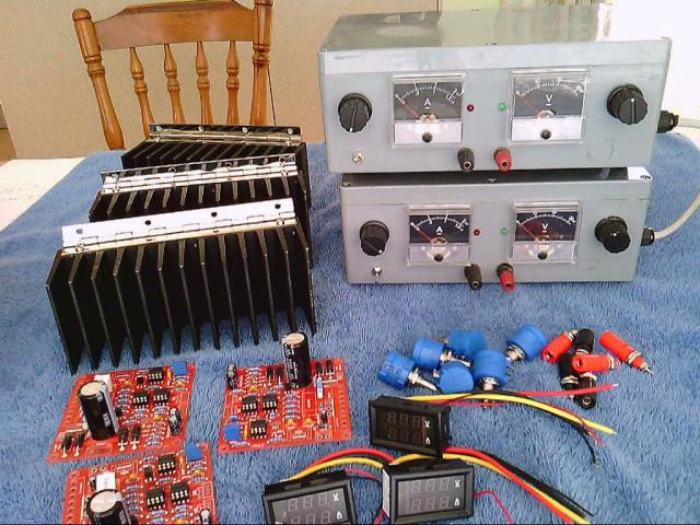 I wanted these to be REALLY accessible inside, and REALLY easy to fix, so the heat sinks are mounted on a hinge and fold right back exposing all the guts. 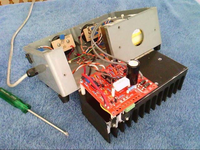 The plastic boxes are the largest size from Jaycar HB-6134 (240 x 160 x 80) and the kit PCB just mounts vertically inside exactly with zero wiggle room. These particular boxes have been recycled and have a few extra holes here and there. Panel meters were salvaged from a dead power supply, so the next three will have digital panel meters. Transformer also comes from Jaycar, its MM-2015 (24v/30v 100Va). I did try another 24v transformer I already had here, but the output voltage under no load was a bit high and the power supply over input voltage protection kicked in. That may be a problem, but the Jaycar transformer works fine, and the exact equivalent from Altronics should work just as well. Heatsinks are Inspire grid tie heat sinks cut down to 80mm height. An 80mm computer fan will go onto that eventually, maybe even two. Cheers, �Tony. |
||||
| Ralph2k6 Senior Member Joined: 24/09/2017 Location: AustraliaPosts: 129 |
Very tidy! I see the IC's are on sockets too, nice. Would you consider using spare old DC plugpacks for supply instead of transformers? Ralph |
||||
TassyJim Guru Joined: 07/08/2011 Location: AustraliaPosts: 6509 |
Thanks for the circuit diagram. My kit arrived this week after 2 months on the slow boat so it's off to the shed to find a suitable transformer and case... Jim VK7JH MMedit |
||||
Madness Guru Joined: 08/10/2011 Location: AustraliaPosts: 2498 |
An old laptop supply would be even better with the higher current. I have one here that is 24V 9A. There are only 10 types of people in the world: those who understand binary, and those who don't. |
||||
| Warpspeed Guru Joined: 09/08/2007 Location: AustraliaPosts: 4406 |
That should work, but the current may be a bit limited. The great thing about these kits is that you can make a few changes here and there to suit your own needs. Yes definitely IC sockets, and screw terminal block for the big mosfet. I mounted the driver transistor on the main heat sink as well, also into a socket. That was before I decided to go to a mosfet. The next three will just have the driver transistor soldered onto the main board without its own small heatsink. There are two resistors that can get pretty hot. R21 the 2K2 1 watt dc bleeder resistor, and of course R20 the five watt current shunt. That really suffers at three amps. I spaced both off the board on ceramic spacers. 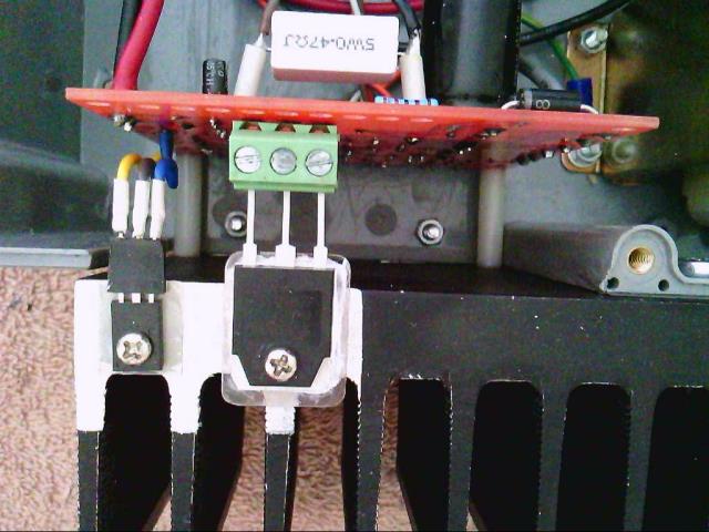 The mosfet legs hold the top of the circuit board, two long 3mm screws with plastic spacers at the bottom can quickly release the whole board if you need to solder underneath. Its an absolutre joy to work on ! One final tip. If you decide to use these plastic boxes, the inside is studded with projecting bosses which usually just get in the way. I used to grind these away with a dremmel, but that is an awful job. One hit with a hammer and a sharp wood chisel knocks those suckers clean off. Magic, and it only takes one second to do. 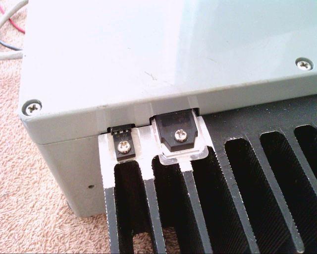 Cheers, �Tony. |
||||
| Tinker Guru Joined: 07/11/2007 Location: AustraliaPosts: 1904 |
OK here is the promised drawn schematic, construed from Warpspeed's sketches. Can you please double check it and tell me of any mistakes so I can update that schematic. Also, if you feel any other info that should be shown too. 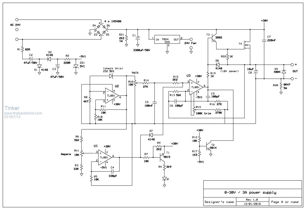 This should make it easier to work on this board. Klaus |
||||
| Warpspeed Guru Joined: 09/08/2007 Location: AustraliaPosts: 4406 |
Perfect Klaus ! And a very neat job too. Just a reminder for everyone, this needs to be used in conjunction with the board layout sketch, because there are no component designators on the PCB itself. Without that, it would be much more difficult to navigate, because there are many components of identical type which rather confuses things.  Cheers, �Tony. |
||||
| Tinker Guru Joined: 07/11/2007 Location: AustraliaPosts: 1904 |
Tony, are you telling me that you found no mistakes? That would do my ego no good at all  . .The little trimpot, set it for zero output with both pots at minimum? Klaus |
||||
| Warpspeed Guru Joined: 09/08/2007 Location: AustraliaPosts: 4406 |
That trim pot RV3 does not appear to have any effect at all that I can see, even with the voltage pot set at minimum. I have not investigated that any further. What does effect the voltage and current maximums is the 10.2v internal voltage reference (U2 pin 6) which can vary rather a lot because the 5.1v zeners supplied in the kit are not particularly accurate. The other thing is that R20 is just a standard wire wound resistor, not a precision current shunt. The combination of a not too certain 10.2v reference and a not too certain 0.47 ohm R20 means the maximum achievable current may end up being quite a bit more or less than 3.0 exact amps. But despite all of that, it behaves very well at startup and shut down, and the dynamic response to step load changes is pretty good. Cheers, �Tony. |
||||
Madness Guru Joined: 08/10/2011 Location: AustraliaPosts: 2498 |
Klaus you have done a nice job there, any chance that you could print it to a PDF and attach the file? There are only 10 types of people in the world: those who understand binary, and those who don't. |
||||
| Tinker Guru Joined: 07/11/2007 Location: AustraliaPosts: 1904 |
Ha, apparently none of you bothered to check this schematic! There is a glaring error on the above drawing, which I copied from warpspeed's sketch, unfortunately. Can you spot it? So, please disregard the above schematic, I'll attach the corrected one below. Madness, sorry, can't do PDF. Irfanview, which I use to convert the original bitmap, refuses to save in .pdf format. What's wrong with the .gif file anyway? Can't you just print it out? A couple of other items relating to the component designations warpspeed posted. I did a *very* thorough check by comparing my schematic to the PCB tracks and found the following: T3, ECB should be flipped to read BCE if this transistor is mounted on top of the PCB as per silk screen. RV1 & RV2, label the pot leg opposite the silkscreen A & V as cw (clockwise) to get the pot rotation correct if the plug in extension wires are used. 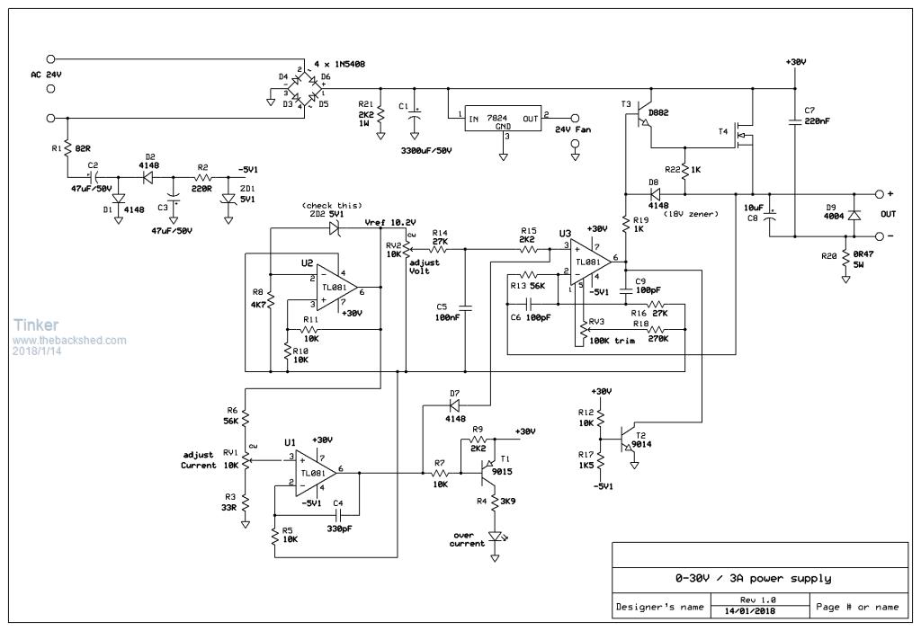 Klaus |
||||
| Warpspeed Guru Joined: 09/08/2007 Location: AustraliaPosts: 4406 |
Well this is something I have never seen before, its quite unique. Klaus is quite right, but would you believe the 2SD882 data sheet I was using is wrong. They have numbered their pins backwards, 321 instead of the usual 123. If you cannot believe a data sheet, what can you believe ? http://www.st.com/content/ccc/resource/technical/document/datasheet/94/f8/66/07/d9/c8/40/55/CD00062867.pdf/files/CD00062 867.pdf/jcr:content/translations/en.CD00062867.pdf 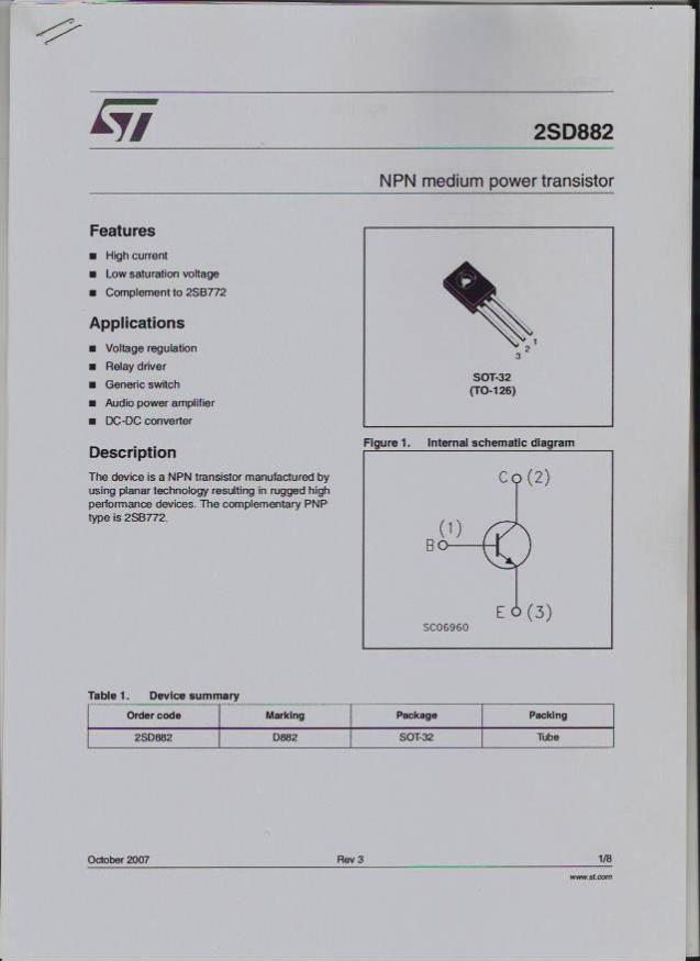 I looked at this circuit for a long time, printed out the transistor data sheets and tried to reverse engineer the whole thing. So I just assumed the data sheet had the right connections. As for the safe operating area of the 2SD1047 output transistor, see Figure 2 in the data sheet: http://www.st.com/content/ccc/resource/technical/document/datasheet/b3/86/80/4e/89/45/4b/6d/DM00026462.pdf/files/DM00026 462.pdf/jcr:content/translations/en.DM00026462.pdf Thirty volts and three amps takes us right up to the maximum for dc operation. Its not a safe design. It has its toes hanging right over the abyss. Cheers, �Tony. |
||||
Madness Guru Joined: 08/10/2011 Location: AustraliaPosts: 2498 |
Klaus to create a PDF normally you print to a PDF printer driver which makes the file. Later versions of windows have this built in, just print the document and select Microsoft Print to PDF, if you are using some other operating system there will be a similar procedure. There are only 10 types of people in the world: those who understand binary, and those who don't. |
||||
| Tinker Guru Joined: 07/11/2007 Location: AustraliaPosts: 1904 |
Tony, I looked up that datasheet too but see nothing wrong there with the pins. Perhaps the confusion lies with the transistor orientation, it has the heat sink surface toward the PCB edge, not facing in as the datasheet picture shows. Gary, perhaps you are not familiar with the Express PCB schematic program I use to draw this. It lets me print to my printer and does that automatically as soon as I hit the 'print' button. There is no file I could access (AFAIK)ready for me with that process. The only way I can save the document other than a .sch file is exporting it as a bitmap. Klaus |
||||
| The Back Shed's forum code is written, and hosted, in Australia. | © JAQ Software 2026 |