
|

|
Forum Index : Microcontroller and PC projects : SSD1963 Board in Sprint Layout
| Author | Message | ||||
| Mixtel90 Guru Joined: 05/10/2019 Location: United KingdomPosts: 8781 |
The switchers don't seem to care what the input voltage is providing it's within their limits. However, I personally don't like to cascade a switcher off a switcher due to possible noise issues. Sometimes it has to be done though, if it would be a problem having the lower voltage present without the higher one. A linear off a switcher is fine and works well. Mick Zilog Inside! nascom.info for Nascom & Gemini Preliminary MMBasic docs & my PCB designs |
||||
| PhenixRising Guru Joined: 07/11/2023 Location: United KingdomPosts: 1856 |
Was just messing around with the plug-in that I posted earlier in the thread: Paid no attention to design rules, mind but I think I came across a bit of funky routing from GP12? 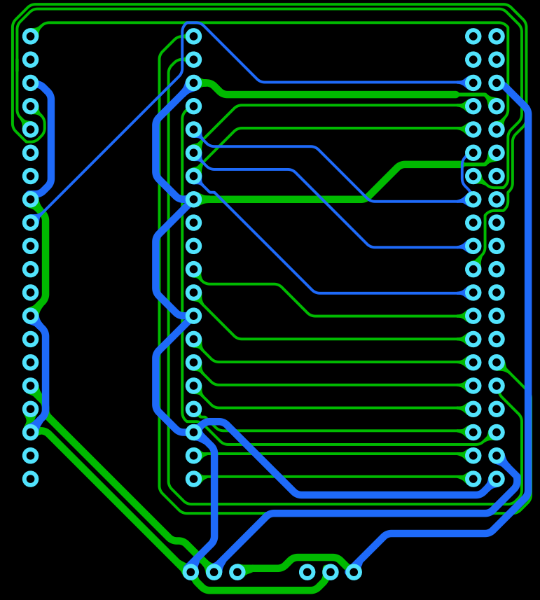 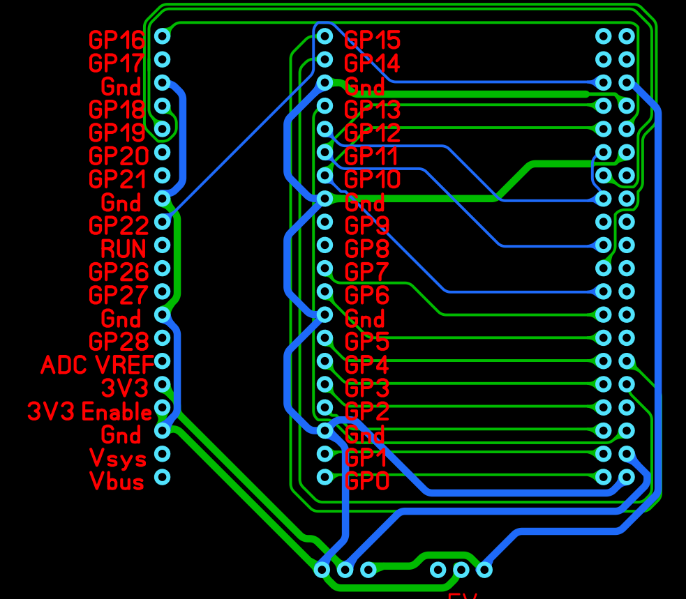 lcd V3-sexed-up.zip |
||||
Bryan1 Guru Joined: 22/02/2006 Location: AustraliaPosts: 1880 |
Thanks for that sexup  Phenix and gotta say it does look a heap better Phenix and gotta say it does look a heap better  I haven't installed those plugin's yet and I will do a bit later. Now when I did a DRC there was 2 tracks going between pad's that were too close. I haven't installed those plugin's yet and I will do a bit later. Now when I did a DRC there was 2 tracks going between pad's that were too close. Yesterday I cut the hole in that box and my feeble attempt at finding screws to hold the LCD down as I did have to cut the posts down to fit the LCD. 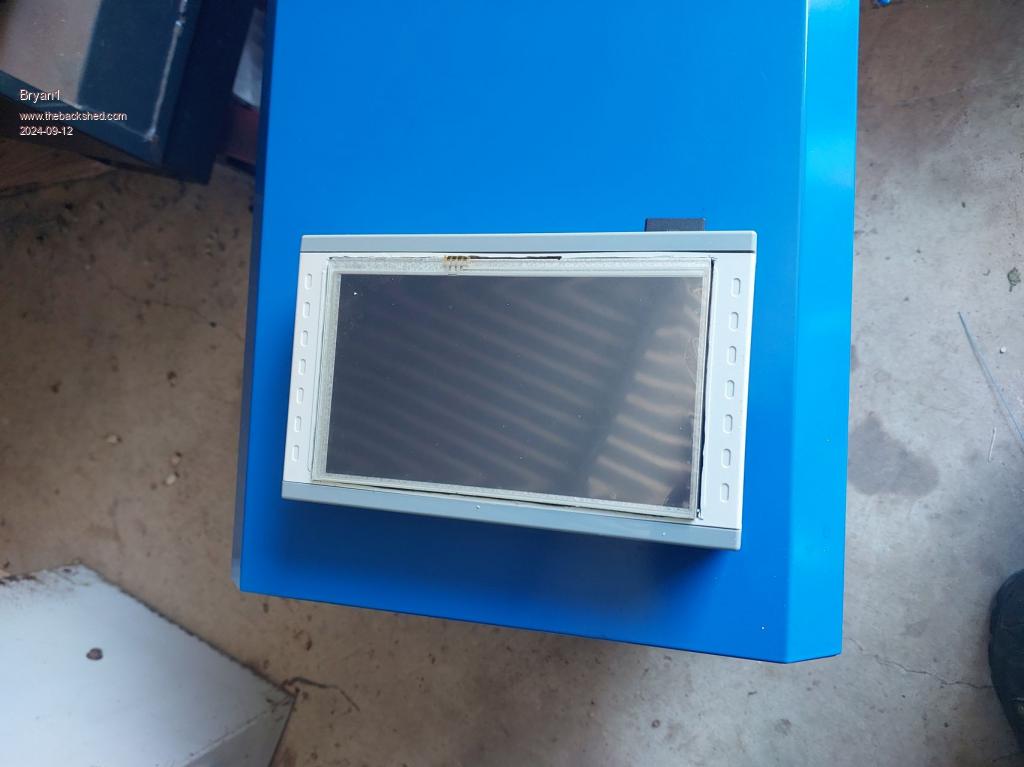 So some loctite 406 soon did the job of clamping the LCD to the box. The slot for the SDCard is already done and on measuring it up the board will be 130mm long X 90mm wide and placed a mm or two away from the back plastic cover so I put in a dinckle connector so the battery can be charged. 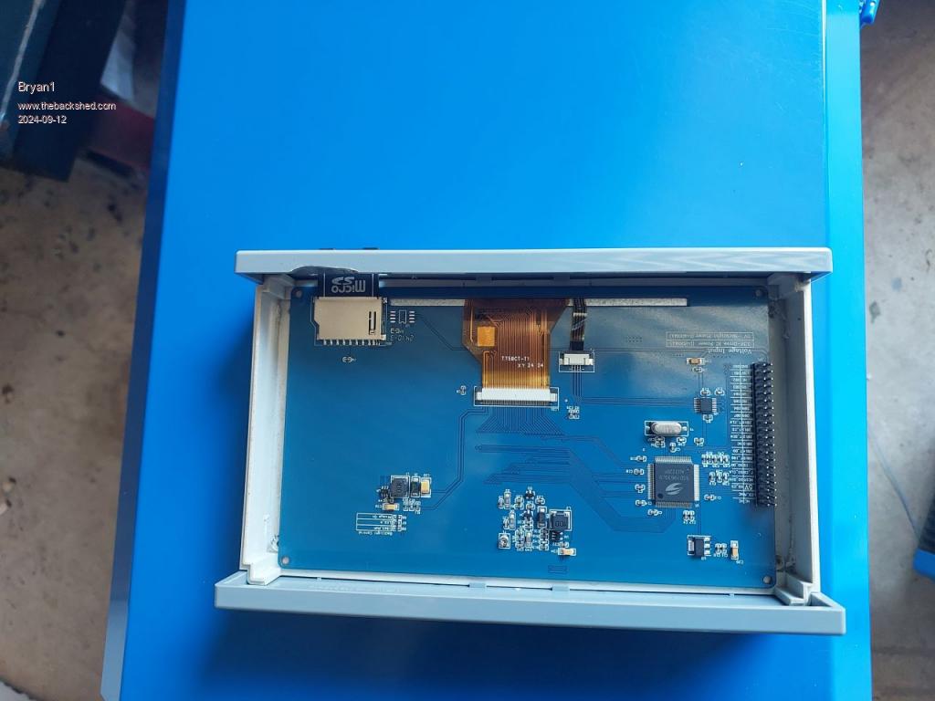 Regards Bryan Edited 2024-09-12 13:17 by Bryan1 |
||||
| Volhout Guru Joined: 05/03/2018 Location: NetherlandsPosts: 5860 |
Hi Bryan1, I noticed you have 2 3-pin connectors on the board. Probably for powering the board. However the pinout on these 2 connectors is different. When there is a good reason to do so (since the cables that plug into them are existing cables) this is okay. But if you ever swap the connectors, you destroy both LCD and Pico. My suggestion is to make the 2 connectors fool proof. Either same pinout (it is fine that one has 3.3V and the other not, as long as GND and +5V are on the right location) -or- make the connectors different, so you can't plug them wrong (i.e. 3 pin and 2 pin ??), or one 0.1" header, the other JST. And preferably alway design with "keyed" connectors (you cant plug in reverse). Regards, Volhout B.T.W: that is a nice build... Very professional to make an interface board from LCD to pico. I usually use "Stan"'s method, and hand wire each connection on a "sea of holes" experimentation PCB. Edited 2024-09-12 16:05 by Volhout PicomiteVGA PETSCII ROBOTS |
||||
Bryan1 Guru Joined: 22/02/2006 Location: AustraliaPosts: 1880 |
G'Day Harm the reason the pin outs are different is to suit the LD1117V3 and the 7805 regulators which I put on before I ordered those switchmode regulators so I will endup changing them. Now once those pins are connected they won't be changed as they will be soldered on to ensure a good connection. Now looking on Grogsters site he does have those genuine HC-12 RF modules so I am thinking of putting one on each one of these I make so they can talk with each other and the picoVGA I'm yet to get. Now as JLCPCB does do 5 off's I am thinking of putting on a sea of holes just so I can get the design off to them. Regards Bryan |
||||
Bryan1 Guru Joined: 22/02/2006 Location: AustraliaPosts: 1880 |
Ok just had a play in Sprint Layout and I reckon this design is close to ready to go.  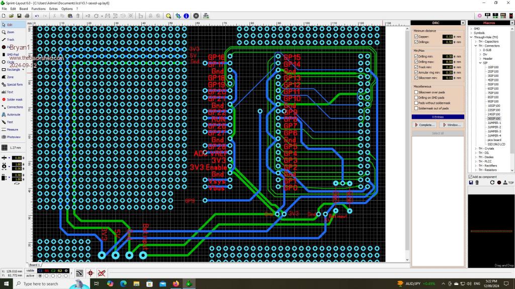 Put in a sea of holes so each project can be expanded and the sea of holes at each edge of the board is for connecting stuff that goes thru the front and rear cover. A smaller board will be made to suit the switchmode modules and the charger module and as shown there is no way the connections can be wrong. lcd V3.1-sexed-up.zip Regards Bryan Edited 2024-09-12 17:54 by Bryan1 |
||||
| Mixtel90 Guru Joined: 05/10/2019 Location: United KingdomPosts: 8781 |
If you make the sea of holes single sided it's easier to de-solder components and re-use it. You don't often need PTH here or the copper plane. You can window that out on both sides so you end up with something like ordinary pad board. You need to switch both ground planes on to see what I mean. Also, watch the hole sizes if you use that 4A switcher. They are big. Edited 2024-09-12 19:21 by Mixtel90 Mick Zilog Inside! nascom.info for Nascom & Gemini Preliminary MMBasic docs & my PCB designs |
||||
Bryan1 Guru Joined: 22/02/2006 Location: AustraliaPosts: 1880 |
Mick the ones I got were the 1.2 amp ones and they aint that big off the pic, anyway I will be soldering wires onto them then soldering the wire to the board so got some flexibility if the box does need to come apart again to add new stuff. Now as far as soldermasks go not quite sure how they work Regards Bryan |
||||
| Mixtel90 Guru Joined: 05/10/2019 Location: United KingdomPosts: 8781 |
Soldermask is used to cover the board. It "masks off" areas so that they won't accept solder. The "Solder Mask" button gives you a view where the areas without solder mask (i.e. are solderable) are highlighted. Often I don't want vias to be solderable, so in that view click on them and they "switch off". Ground planes Along the bottom of the screen there are five (or seven) boxes that change your layer and switch it on and off. Just to the right of them is a slightly larger box with a pad in it. Clicking that toggles the ground plane copper for the current layer on and off. To the right of that are three boxes. The upper one sets the width of the blank area surrounding the traces and pads. The two bottom boxes select rectangle or freeform for ground plane cutout. If you click the rectangle one then click on the visible groundplane somewhere you can drag out a rectangle in which there is no groundplane. Soldermask is used to cover the board. It "masks off" areas so that they won't accept solder. The "Solder Mask" button gives you a view where the areas without solder mask (i.e. are solderable) are highlighted. Often I don't want vias to be solderable, so in that view click on them and they "switch off". Mick Zilog Inside! nascom.info for Nascom & Gemini Preliminary MMBasic docs & my PCB designs |
||||
| PhenixRising Guru Joined: 07/11/2023 Location: United KingdomPosts: 1856 |
@Mick...I wasn't sure if Bryan was wondering how to make the holes single-sided, per your suggestion. |
||||
Bryan1 Guru Joined: 22/02/2006 Location: AustraliaPosts: 1880 |
Mick the reason I made the sea of holes double sided is on the bottom layer there isn't much room height wise so larger parts can go ontop the board where there is more room. Also with it being double sided it will make it easier to solder tracks on the sea of holes. I do have to go down to town today as I scored a i7 SFF computer for my wife for $40 so later when I get back I'll have another play. It would be great to get this design finished so I can get it off to JLCPCB as time wise everything will turn up around the same time. Regards Bryan |
||||
Bryan1 Guru Joined: 22/02/2006 Location: AustraliaPosts: 1880 |
G'Day Guy's, Well got some spare time and falling over the first step, the otherday I tried to get that ILI9341 LCD working so setup the pico as per the manual. Well the LCD was just throwing a flickered screen and the bubbles did popup once or twice. Now forward to today disabled the ILI9341 and tried OPTION LCDPANEL SSD1963_7, L, GP15, GP14, GP13 Then got this Now I did reflash the uf file and when I did that option list the SPI and TOUCH are still shown to be set ? option list PicoMite MMBasic Version 6.00.00b4 OPTION SYSTEM SPI GP18,GP19,GP16 OPTION TOUCH GP12,GP11 > OPTION LCDPANEL SSD1963_7, L, GP15, GP14, GP13 Error : Pin 21/GP16 is reserved on startup > OPTION SYSTEM SPI DISABLE Error : In use > OPTION TOUCH DISABLE > option list PicoMite MMBasic Version 6.00.00b4 OPTION SYSTEM SPI GP18,GP19,GP16 > option lcdpanel ssd1963_7, L, GP15, GP14, GP13 Error : Pin 21/GP16 is reserved on startup > option lcdpanel ssd1963_7a, L, GP13 Error : Pin 21/GP16 is reserved on startup > So not sure what's going here ? Regards Bryan Edited 2024-09-13 15:14 by Bryan1 |
||||
Bryan1 Guru Joined: 22/02/2006 Location: AustraliaPosts: 1880 |
Well lesson learned one can't simply load a new uf file so on reading the manual downloaded the clear flash uf file and ran it. Reloaded the V6 uf and got the LCD, SDCard and Touch all set so now to setup the breadboard and see if I can get this LCD going. > option list PicoMite MMBasic Version 6.00.00b4 OPTION SYSTEM SPI GP10,GP11,GP12 OPTION LCDPANEL SSD1963_5_16, LANDSCAPE > OPTION SDCARD GP22 > OPTION TOUCH GP18, GP19 > option list PicoMite MMBasic Version 6.00.00b4 OPTION SYSTEM SPI GP10,GP11,GP12 OPTION LCDPANEL SSD1963_5_16, LANDSCAPE OPTION TOUCH GP18,GP19 OPTION SDCARD GP22 > Regards Bryan |
||||
Bryan1 Guru Joined: 22/02/2006 Location: AustraliaPosts: 1880 |
Well on reading the manual further a thought came to me about the supported devices so I got onto Ali and have some HC-SR04 ultrasonic sensors and some OV7670 camera's coming. So this first 7"LCD can be used with both of these devices to take a picture to measure and take a length. Then saved on the SDCard and later sent over with a HC-12 to a master pico. Should make for a handy tool just using the supported devices, now with this $10 box only having 40mm of height it maybe a tight fit but a fun project to do. Regards Bryan |
||||
Bryan1 Guru Joined: 22/02/2006 Location: AustraliaPosts: 1880 |
Well JLCPCB did accept my zip file of the prototype board and $17.80 for 5 boards  So all those other parts should arrive around the same time. So all those other parts should arrive around the same time.Only thing at the end of the month I'm taking my daughter over east for a holiday to see my sisters so it will be next month when the fun really starts. So today it's back to the manual for more reading and see if I can get the LCD going on my breadboard. Regards Bryan |
||||
Bryan1 Guru Joined: 22/02/2006 Location: AustraliaPosts: 1880 |
Got an email saying I left out the outline layer off  and with so many holes I had to change it to enin and fixed the zip file to include the outline layer. Gotta say dealing with them is quick and timely and with so many holes I had to change it to enin and fixed the zip file to include the outline layer. Gotta say dealing with them is quick and timely  Now when I redid the zip file silly me forgot to change the dimensions of the pcb and not long after got an email with instructions to setup a JLCPCB payment account. So got it all setup and 5 minutes later my first purchase was in there so they can take that extra $6.70 US for the pcb board dimension change. Anyway my next sprint layout project is going to be that isolated board for my CMM2-CNC project as my fist attempt on strip board was only 2 of the 10 2N35's actually worked with my led setup on the breadboard. Edited 2024-09-14 18:09 by Bryan1 |
||||
Bryan1 Guru Joined: 22/02/2006 Location: AustraliaPosts: 1880 |
G'Day Guy's, Bit of an update those boards from JLCPCB have shipped and yesterday got those 3v3 and 5v buck boost reg's  According to Ali tracking those camera and ultrasonic boards will be here early next week. According to Ali tracking those camera and ultrasonic boards will be here early next week.Got a few jobbies to do to keep in the good books then time to play. Regards Bryan |
||||
Bryan1 Guru Joined: 22/02/2006 Location: AustraliaPosts: 1880 |
Well found some time yesterday to get this all wired up and noway would the lcd work  So thought just leave it for the next day and try again. So thought just leave it for the next day and try again.  Well this morning YAY the LCD lives and found yep the cursor was a small font and upside down so reset the pico and changed the setting only to find the pico led stopped and lost connection on com14. So reloaded V6 after doing a clear flash and found the lcd was a blue font and placed 1/2 way down the screen so changed the setup again only to find the same problem and the third time it did look the same no LCD output then as soon as I set the touch pins the LCD came to life. 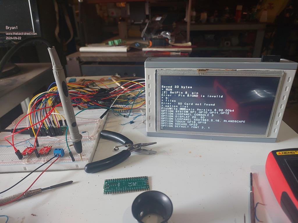 Still need to sort out the SDcard as it wasn't found and decided to do a simple code to read GP8 where I used the simple code out of the manual setpin 8, AIN print pin(GP8) and got the error shown. Got a 10K/4.7K divider and GP8 has 2.5 volts on the pin so why this simple code won't work and soldered pcb pins to those buck regualtors so they fit on the breadboard. Also found as I provided 5 volts to the LCD I had to connect LED_A to 5 volts to get the back light to work. So more fun is on the way as I try and get this setup Regards Bryan Edited 2024-09-22 11:36 by Bryan1 |
||||
| phil99 Guru Joined: 11/02/2018 Location: AustraliaPosts: 3163 |
setpin 8, AIN print pin(GP8) and got the error 1) Pin 8 is not the same as GP8, so to make life easier just use GP numbers. To see the difference type:- print mm.info(pinno GP8) and it will show the pin number. 2) The only pins that can be used for AIN are GP26, GP27, and GP28. Eg. > setpin gp28, ain > ? pin(gp28) 0.7721489621 > The PicoMite Hardware chapter in the manual shows which pins do what. The SD card connections for your System SPI are:- SD_CS GP22 SD_MOSI GP11 SD_MISO GP12 SD_CK GP10 The outputs of touch and the SD card share one input - MISO and sometimes that seems to cause an issue, especially if touch has not been configured. 4.7kΩ pullups on T-CS and MISO sometimes seem to help. Then there is the fussiness of some SD cards. I have one that won't work on System SPI but does work on a BitBanged SPI port on the PicoMiteVGA. No idea what the difference is. All you can do there is try other cards. The maximum size is 32GB and fat or fat32 file system. . Edited 2024-09-22 15:25 by phil99 |
||||
Bryan1 Guru Joined: 22/02/2006 Location: AustraliaPosts: 1880 |
Hi Phill yes I did have the mosi and miso lines around the wrong way and got the error the sdcard wasn't formatted which to me was strange as that is the one from the CMM2. Anyway had a 32gig card which did show up with that one JPG file I had. Finally got the touch going and at first I tried a thin bit of wire only to find it failed with too much error so I tried my fat thumb and it calibrated first time  Now I can read the voltage of the pin using your method but my code just producing zero so a bit of guidance would be nice. dim battery as integer setpin GP26, AIN battery = gp26 ' Get some readings DO ' Read the analog input battery = battery * 3.098 ' scaling for battery voltage PRINT "Battery Voltage: "; battery pause 10000 ' wait awhile LOOP Regards Bryan |
||||
| The Back Shed's forum code is written, and hosted, in Australia. | © JAQ Software 2026 |