|

|
Forum Index : Electronics : Inverter #5
| Author | Message | ||||
| Tinker Guru Joined: 07/11/2007 Location: AustraliaPosts: 1904 |
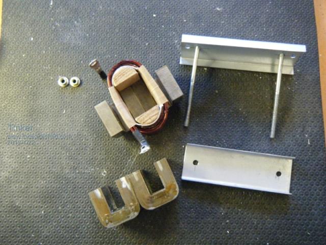
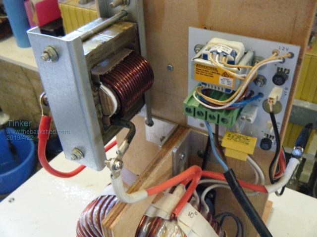
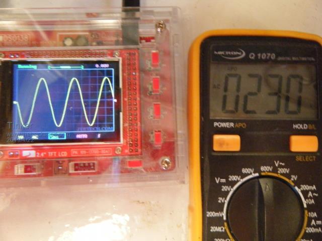
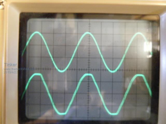
Today my new home made choke got connected and all is well now with my little inverter #5. Here is how the choke looks:  All made from re cycled aerosharp chokes. The C cores from the smaller aero choke converted to an E core. The wire (2.5mm dia.) from a big aero choke for the coil. And the metal clamping brackets from the PCB mounting plate in the aero. The specs: 17 turns of 10 sq mm wire. 0.85mm spacers between the pole faces. Measured inductance was 0.2mH. My calculations show it would saturate at well over 100A peak so plenty of safety margin for that little inverter. This is how its mounted now:  And it works very well, no more distortions. The next pic is the sine wave while powering a 600W load:  I must thank poida here for coming up with this marvelous sine wave generating idea, it looks heaps better than the sine wave from the EG8010 chip. See both waves on the next pic. The top one is the poida sine wave, the bottom one the EG8010 sine wave. As these two inverters were not synced the bottom wave moved across the screen surprisingly fast, hence the 'double' trace.  So there must be a bigger frequency difference between the nano inverter and the EG8010 version. I did look at the sine traces of the two EG8010 based inverters I have here, which are running independently, for comparison. While both had the crappy sine wave, like the bottom one above, the out of sync drift was very slow, it took many minutes to be 180 degrees out. The nano inverter was 180 degrees out in just a few seconds. I do not have accurate frequency measurement here but my clamp meter does Hz and measured 50.1Hz at the nano inverter. IMO, a choke like the one I made above is heaps better than any of the ferrite version I had experienced with. This single nano inverter must have the active filter fitted. It will run without it but the wave form is not as good. The nano inverter now has a better AC voltage regulation than my EG8010 based inverters. Everything is now ready to test the two inverter syncing idea. I will start another topic when the results are in. Klaus |
||||
| wiseguy Guru Joined: 21/06/2018 Location: AustraliaPosts: 1267 |
Klaus - that looks much better - I also like your c to e choke conversion and the resultant waveform. I was on the verge of getting some software created to achieve what Poida has created and he sure saved me a lot of trouble too. I got to the point that I didnt want to deal with the 8010 and its method and issues of creating sine waves and needed another way forward. I too have built an efficient nano sinewave inverter (mine 300W from 12V) which I am currently packaging for use when travelling and camping. I will soon (1 -2 weeks) inherit a decent battery bank from a failed solar installation that has been replaced but not collected, I believe just one cell is either not charging properly or is faulty - either way I'll deal with it as appropriate. I have been considering a different approach to achieving higher currents using cheap $5 PCbs instead of copper wires and solder wick. I'm interested to hear your comments and feedback good or bad. 100 x 100 boards are all $5 regardless of thicknss from 0.6 to 1.6. Suppose we get 2(3) PCBs 100mm x 100mm but 0.6mm or 0.8mm thick and double or triple them up, we will end up with 2 x 0.8mm PCBs (4 x 1oz layers) total thickness 1.6mm, or 3 x 0.6mm PCBs (6 x 1 oz layers) total 1.8mm thick, but with much greater current capability. There will need to be 2 or 3 designs I think as they need to be a mirror to the facing layer but compared to getting 2oz or 3oz PCB's costing either $48 or $200 for 2 or 3 oz, I reckon its worth exploring. Essentially it is a discrete 4 or 6 layer PCB stack and each layer is 1oz and uninsulated from the facing layer so 3 PCBs is equivalent to up to 6oz - yes I know you should derate internal layers. The 3 layer approach is probably better suited to smd parts on the top pcb & with higher current FETs, connectors, capacitors etc using the through holes. For your power pcb design the internal facing layers could all be the same as the solder side layer but the signal traces are only needed on one layer - the solder side? for instance leaving more area for current tracks in the internal facing layers - also more appropriate though when multi FETs and higher overall currents are used. If at first you dont succeed, I suggest you avoid sky diving.... Cheers Mike |
||||
| hary Regular Member Joined: 15/04/2019 Location: FrancePosts: 89 |
Hi there. I don't want to disturb, but I've been interested about what's going on in here about inverters. I then read a lot of post, but now feel a little lost. I've first seen Ozinverter with its own control board and power board, then some promising stuff about the EGS002 control board. Then there were theses Warpinverter and Madinverter, some with Arduino nano1 and nano2 control board etc, etc ... Even this syncinverter. When I first saw Ozinverter from back 2015-2016, I was very enthusiastic, thinking that at these days a definitive working version would work fine. Today, reading all these threads, I'm a little disappointed and lost. Is there a version that works, I would say out of the box ? I love what's happening here, lots of search, etc. Unfortunately, I'm not a genius as you are. I could probably copy what you're doing, and learn some from it, but no more Any advices would be very appreciated. PS : I have some old UPS kept to an hipothetic time I could do something from them. Maybe now ? |
||||
| wiseguy Guru Joined: 21/06/2018 Location: AustraliaPosts: 1267 |
Hary you are re-visiting this site during a time of new developments and many shared ideas and upheaval. The dust hasnt settled yet but the Warp inverter is a reliable robust unit with much promise to work out of the box - but multiple transformers with some unusual turns ratios and extra circuitry is required to create it and the final design is still evolving from a lot of work from a few main contributors Mack, Warp & Poida. (If I missed someone else sorry) The EG8010 Oz inverters have demonstrated huge reserve power and some here have built quite reliable units, whilst some others have struggled a bit to make them as reliable. The advice given to you earlier by Mark suggesting a Nano inverter controller and a Mad style Power PCB is probably a good way forward IMO at this time but it is not quite at the one size fits all with complete parts lists and build instructions, but I think this will happen in due course. If you want to build an EG8010 version, maybe Clockman also from France could help you with a kit and full instructions and some local mentoring and support ? If at first you dont succeed, I suggest you avoid sky diving.... Cheers Mike |
||||
| Warpspeed Guru Joined: 09/08/2007 Location: AustraliaPosts: 4406 |
Its a very long complicated story Hary. The Oz inverter was absolutely brilliant, and still is, but it gets more difficult to build successfully as the power level increases. Some people have been more successful than others, and there has been a great deal of development and many different ideas tried in attempts to solve all of the various problems that have arisen. The problems range from deep suspicions about Chinese EGS boards, and the EGS software, as many of these boards come with components deleted or changed. Problems driving multiple very large mosfets as people keep adding more and more extra mosfets to raise the power level. Problems with the current limit circuitry, and voltage regulation. A great deal has been learnt about the magnetics, how to reduce idling power and reduce distortion, and problems with layout and spurious noise causing software crashes and blow ups. A great deal of effort has also gone into developing our own local home brew software and firmware with greater functionality and greater reliability. Its not then all a complete mystery like the offerings from China. Some of those Chinese chips may be counterfeit and have dodgy imitation software, who knows ?? The whole home brew issue seems to be fraught with problems, and for many Forum members has not turned out to be the simple straight forward build that was initially hoped for. Many Forum members have neither the sophisticated test equipment, or the electronics experience to solve these blow up problems. The Warpverter is a totally different concept altogether to high frequency PWM, but at this very early stage has not been proven to be a solution for all the known frustrations of very high power high frequency PWM. An Oz type of PWM inverter is far better suited for lower power levels, and many people have built prototypes that run very well with only four mosfets, but blow up when extra mosfets and far higher power levels are attempted. The Warpverter uses more parts and will be larger and more expensive to build, but because it switches at a much slower rate, (about 460 times slower) many of the high frequency problems with very fast switching PWM just do not occur. A Warpverter is also going to be much easier to scale up in power level without the noise and criticality of layout that plagues high power high frequency PWM. No critical chokes or transformer tuning required either. And the performance will be about the same regarding idling power and full load efficiency. Response to sudden load changes (light flicker) should be better. But its all a very new concept. Several Forum members are now in the process of building their own Warpverters. Just be patient and see how that all goes before jumping in yourself. I have built several of these successfully over the years, and they have all been very tough and forgiving, and for those reasons much more suitable for people to copy as a project. The only complication is winding the four transfomers, which is a formidable task, but its pretty straightforward, just a lot of work. If you can get that far, the rest is very straightforward and should be easy. Cheers, ĀTony. |
||||
| Tinker Guru Joined: 07/11/2007 Location: AustraliaPosts: 1904 |
Interesting idea Mike but I see a big problem. When they do commercial multilayer boards there are usually a gazillion tiny vias in the power planes to link the internal tracks to the external ones by plate through holes. You cannot do plate through on a stack of finished boards so how would you effectively link the inside layer to the outside layer? Even double up tracks on top and bottom of a single PCB were a problem as I had discovered. Hoping to double the current capacity of a wide track by doing that and added a few through plated vias plus the plated through hole at the connector pin. It blew the track at the top side where the shared current came through the single plated hole at the connector. The tracks were OK for 500-900Watts or so but a sudden load of 1000W was too much for them. So I will stick to the solder lug addition right at the terminal pad (which has to be narrow) and beefing the track with solder wick, which is a cheap and working solution. Klaus |
||||
| Solar Mike Guru Joined: 08/02/2015 Location: New ZealandPosts: 1203 |
Vias are only good for 500ma or so, thus you need 100's of them to allow proper current sharing, easier to do as you suggest, add extra copper (wire or bar's) adding heaps of solder is less effective as its conductivity is 1/10 that of copper. Cheers Mike |
||||
| hary Regular Member Joined: 15/04/2019 Location: FrancePosts: 89 |
I migh tbe wrong, but I think the inverter with nano control board has nano1 and nano2 (2 nanos) Are they both dedicated to the same task, or do they have different task and sketches ? Might be not the right place to ask that kind of question ? |
||||
renewableMark Guru Joined: 09/12/2017 Location: AustraliaPosts: 1678 |
hary, no one is going to race out with a silver platter with a perfect solution to your needs. You'll need to read through the site and evaluate the different options. All the information is here, you just need to read it. Everyone's requirements are different, so each build may suit some and not others, that's something for you to decide. Start by reading all of this thread Cheers Caveman Mark Off grid eastern Melb |
||||
| Tinker Guru Joined: 07/11/2007 Location: AustraliaPosts: 1904 |
You are correct, it is NOT polite to hijack somebody else's topic with unrelated questions. Please start your own topic and do, as has been suggested, read as much as you can on this forum. You will be surprised to find the answers to your questions have been already answered long ago. Klaus |
||||
| wiseguy Guru Joined: 21/06/2018 Location: AustraliaPosts: 1267 |
Thanks for the response Klaus. I'm not clear exactly what you did to beef up the current in your tracks - I dont propose getting the current to pass to other traces with vias. Here is a handy little calculator for current capability of a track based on the oz rating (trace thickness), width of tracks and internal/external trace - and temperature rise above ambient - I have used it for years 2019-04-23_232416_TrAMP.zip For 2 sided only PCBs, dont forget to change the default internal trace tick box to external trace when checking temperature rise or it looks a lot worse than it really is. I am suggesting essentially doubling tripling or quadrupling the cross sectional area of the current path routes - I believe ohms law still works and the current will be halved quartered etc for extra trace/s. The FET leg or connector leg carries the bulk current & passes the current to the various layers via the soldering at the plated through component leg holes ( ok the iron would need to be a bit hotter ). I do intend to try this as I believe it will work fine for higher current capability on the cheap. There is not really a need for extra vias along say 2 equal traces that should each carry an equal fraction of the total current. You are correct in that passing high current between layers does need a heap of vias if a low impedance path (component leg) is not available to exploit. I received the vertical mount, single in line pins, mains input, isolated 12 & 15V supplies tonight from Ali. They are a bit different to the horizontal mounted opto feedback types. They are a primary regulated type - they use the auxiliary run winding which is proportional to the output voltage to regulate the control IC - it is not obvious yet what I need to do but I will trace it out soon. I will also check start up voltage etc - do you want me to share the results here or should we start a new thread for little isolated supplies ? If at first you dont succeed, I suggest you avoid sky diving.... Cheers Mike |
||||
| Tinker Guru Joined: 07/11/2007 Location: AustraliaPosts: 1904 |
OK on your current sharing tracks. So you relay a good solder contact to all internal layers at just one pin? Never tried that, let me know how that works. I can see a challenge laying out mirror images of tracks there, perhaps you PCB program has some trick for that. I use this program and one other I found on the net to calculate PCB track current. I'm still waiting for the little supplies you have just received. Can you tell me if a right angle header pin strip, with 0.1" pin spacing, would align with the input & output holes without having to cut the strip? I intend to have these supplies to plug in on the diver PCB. And yes, I'm very interested how you get them to output 15V. I received the boost module today so its no problem to feed the modules with 60V from my battery if they do not start up at 48V. Klaus |
||||
| wiseguy Guru Joined: 21/06/2018 Location: AustraliaPosts: 1267 |
I have some bad news, the input 2 pins are 0.2" spacing the output 2 pins are 0.1" spacing but the input and output pins do not all line up on a 0.1" grid. The pins are also rather short at ~ 3.6mm length of pluggable pin - what dunderhead designed and specified this device...... apart from that its perfect  (the strip will need to be cut) & I think you will need to use a different right angle header pin - I reckon just solder it to the PCB - they'll never fail will they ? (the strip will need to be cut) & I think you will need to use a different right angle header pin - I reckon just solder it to the PCB - they'll never fail will they ?You learn something every day if you're lucky - been dealing with digikey for years and never knew they had that track calculator. If at first you dont succeed, I suggest you avoid sky diving.... Cheers Mike |
||||
| Tinker Guru Joined: 07/11/2007 Location: AustraliaPosts: 1904 |
Thanks for that Mike. I knew from their drawing about the 0.2"spacing on one side, just could not figure out from the drawing they had the in between pin row spacing. Oh well, I'll cut the strip. Just as well I did not yet send the PCB gerbers away, better wait until I get my module order in - should be soon anyway. Here is another PCB track calculator for you. Klaus |
||||
| wiseguy Guru Joined: 21/06/2018 Location: AustraliaPosts: 1267 |
Sorry Klaus, I should have given you the measurement between the closest input & output pins. This is 16.5mm centre to centre. or 0.65" If at first you dont succeed, I suggest you avoid sky diving.... Cheers Mike |
||||
| wiseguy Guru Joined: 21/06/2018 Location: AustraliaPosts: 1267 |
Klaus, these little power supplies are excellent. I tested a 12V & a 15V unit. They both start at 29V (with either polarity on the input  of course you gain another volt or two lower startup if you bypass the bridge but I think this is unnecessary for 48V. of course you gain another volt or two lower startup if you bypass the bridge but I think this is unnecessary for 48V.Running at 30V I could easily pull 100mA from the 15V supply and its output stayed rock solid. I am lazy, I didnt draw out the circuit, its very similar to the application note, I just tried a resistor in parallel with the lower sense resistor a value of 120K & it raised the voltage to 14V. Although not tried 100K should be close to 15V.  The resistor is at the bottom of the picture, the one closest to the input connector lowest pin, on the other side of the plastic pin header. The two components above this resistor are all in parallel, the lowest one is a 270K then a capacitor and then a 5K1 resistor. You just add the 120K resistor in parallel with one of these 3 components. Or remove the 270K and use an 82K - if you are still in touch with Gaspo he might have better tools and eyesight.... Or you could solder a small 120K axial resistor between Pin8 and pin2 of the ic (I would recommend a 1/8W resistor with the skinny leads). Or you could put up with 12,2V. As you can see there are a few ways to skin this cat. If at first you dont succeed, I suggest you avoid sky diving.... Cheers Mike |
||||
| Tinker Guru Joined: 07/11/2007 Location: AustraliaPosts: 1904 |
Excellent work Mike, that saved me a lot of trouble identifying parts. I will have to boost the output to 15V as that is the low end of the supply range the opto drivers in warpspeeds design can accept. I see you fitted right angle pins, that looks very neat and I think I'll copy that  . .Now I just have to wait until the modules I ordered turn up. Klaus |
||||
| wiseguy Guru Joined: 21/06/2018 Location: AustraliaPosts: 1267 |
I bought mine Here They already have the right angle pins fitted. (looks neat cause I didnt do it )  They were 90c US each. I will try to confirm the exact resistor value for 15V tomorrow. If at first you dont succeed, I suggest you avoid sky diving.... Cheers Mike |
||||
| Tinker Guru Joined: 07/11/2007 Location: AustraliaPosts: 1904 |
Just looked at that link to aliexpress. It appears these modules are now available with 15v output - Wish I had known that before I ordered them  . .Klaus |
||||
| Warpspeed Guru Joined: 09/08/2007 Location: AustraliaPosts: 4406 |
Just a couple of random thoughts.... Calculating full load currents, and working out suitable track widths at various copper weights can be fine. Until the first time it goes bang. Fault currents can be many times the expected full load current, and it may explode the tracks off the board. Klaus's technique of solder lugs and solder wick is excellent. Its not just the extreme short term fault carrying ability, but the thermal mass that allows the mosfet legs to explode safely, while causing zero damage to the board. So don't think so much in terms of so many amps of full load current, but will it survive a dead short until the short circuit current clears itself to an open circuits somewhere off the board. These little microcontroller Nano thingies open up enormous possibilities. But they are very unlikely to use an expensive quartz crystal, more likely a ceramic resonator. The clocking frequency may have considerable variation between boards and the frequency drift with time and temperature. And so will the 50Hz inverter output frequency. This may or may not be a problem for you. Some smart appliances, and mains driven clocks, use the 50Hz supply for time keeping, and any inverter frequency error will be cumulative. The grid frequency is long term time corrected, but an inverter is not. Cheers, ĀTony. |
||||
| The Back Shed's forum code is written, and hosted, in Australia. | © JAQ Software 2026 |