
|

|
Forum Index : Electronics : Inverter # 4
| Author | Message | ||||
| Tinker Guru Joined: 07/11/2007 Location: AustraliaPosts: 1904 |
Well, I hope it replaces this: 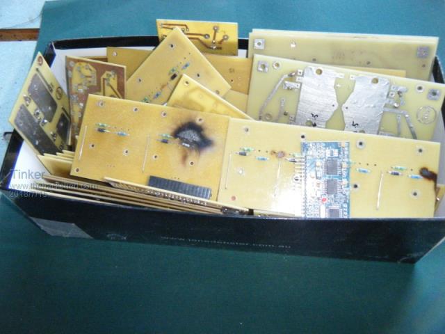 All of these boards are the leftovers of my earlier inverter build experiments  Now I have a design that works but could, perhaps, take a little refinement here and there. If nobody did any experimenting we would not have this do it yourself inverter building anywhere near where it is now. Klaus |
||||
Madness Guru Joined: 08/10/2011 Location: AustraliaPosts: 2498 |
Very true Klaus, I am happy enough with mine to move on to other things. There are only 10 types of people in the world: those who understand binary, and those who don't. |
||||
| Tinker Guru Joined: 07/11/2007 Location: AustraliaPosts: 1904 |
Now for another installment: There is a requirement to provide a 12 and 5 Volt supply from the battery bank so the inverter can start up and run. One method is to use a zener diode shunt regulator. Its the simplest way but dropping from up to 60 Volt to 12 is a big task for a zener diode shunt regulator. Since we can now buy very cheap and compact DC/DC down converters, I prefer to use this method. Madness posted a while ago a link for 90V to 12V/3A down converters and I had ordered two units (one a spare). When it arrived I found it was up to the task and almost tiny physically. In fact, I could fit it into the smallest black snap together box that Altronic has in their catalogue. 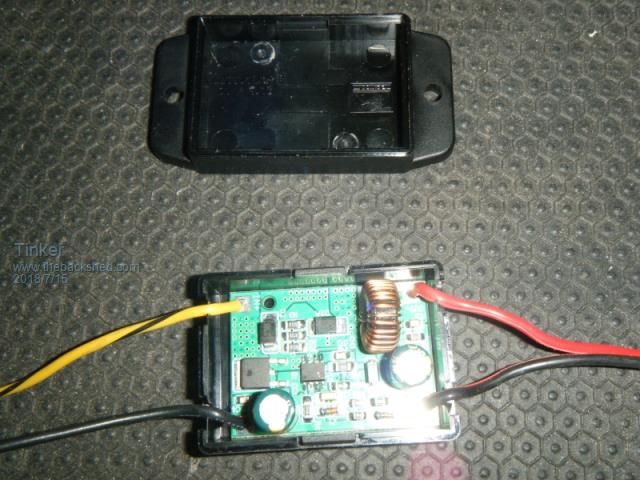 All the box required was to carefully drill out the two board mounting posts inside (see picture) and it was a perfect fit. There are even 4 little knockouts for the wires to emerge. Completed it looks like this. 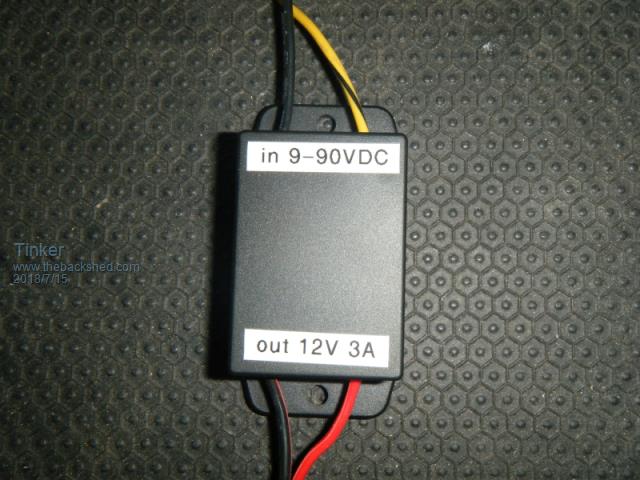 Another useful item, for testing the completed inverter, is a modified battery lead for it. 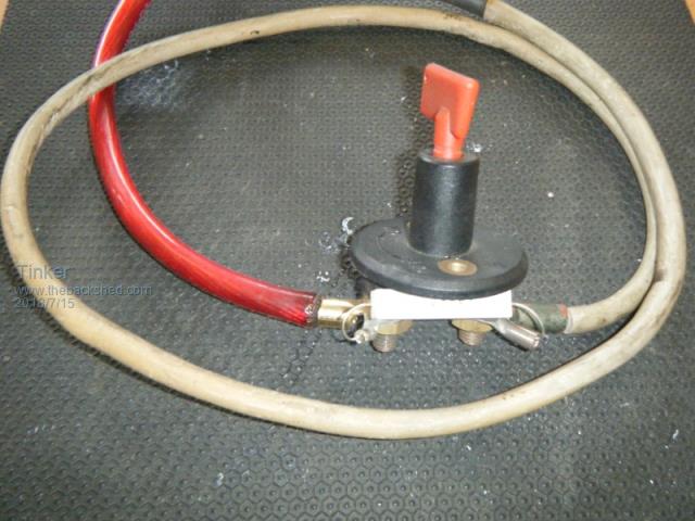 This inexpensive high current key switch has the contacts bridged with a 22 Ohm/10 watt resistor. The red key is removable in the 'off' position. The cables have a welding cable clamp on one cable end end and a solder lug on the other cable. The idea is to *always* connect the to the battery terminal while the key is out. That way the big capacitors slow charge and when fully charged the key is inserted and turned on for full inverter power. An important proviso: The key must *never* be used to turn off the DC under load - it is not designed for that and would weld the contacts if one tried that with a decent load. Always shut down the inverter first with the 'off' switch (pin 6 EG8010). Now I required some method to keep all the parts (heat sinks, toroid, PCB's etc. tidy in place while still being able to access everything easily. So I came up with this backbone idea: 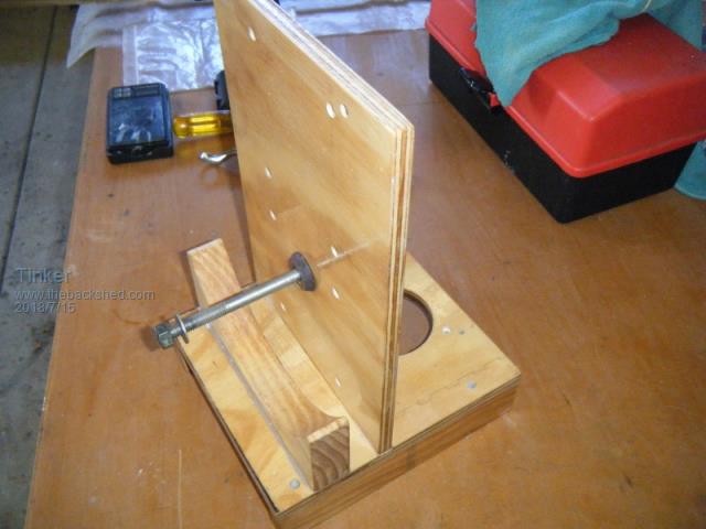 Its made from strong 12mm plywood and easy to construct. The screws for the 'live' heat sinks were recessed countersunk to avoid accidental contact by parts on the other side of the upright board. This backbone also locates the heatsink in an upright position for maximum heat convection. Plus there is a 80mm computer fan at the bottom for extra cooling at high power testing. To be continued. Klaus |
||||
Madness Guru Joined: 08/10/2011 Location: AustraliaPosts: 2498 |
I have had some issues with spikes at turn of those power supplies Klaus, it is a good idea to put a Zener diode across the output. There are only 10 types of people in the world: those who understand binary, and those who don't. |
||||
| tinyt Guru Joined: 12/11/2017 Location: United StatesPosts: 556 |
I used those power supplies but messaged the vendor for 18V output, they provided 17.6V which is good enough for me. They already have a zener at the output but I don't know the zener voltage, so to minimize spikes/noise, I dropped down the output to 16V, 12V, and 5V with linear regulators, hopefully to filter out the spikes/noise. @Klaus, I bought similar high current key switches, thanks for the tip on how to power off. I am guessing they are only rated for 12/24v, so the need for the special power off procedure? |
||||
| noneyabussiness Guru Joined: 31/07/2017 Location: AustraliaPosts: 527 |
power supply This one has multi taps.. I think it works !! |
||||
| wiseguy Guru Joined: 21/06/2018 Location: AustraliaPosts: 1267 |
Caution advised - that particular one is not fully isolated -IN is connected to GND out. If isolation is not required it appears to be a good little low cost solution. If at first you dont succeed, I suggest you avoid sky diving.... Cheers Mike |
||||
| Tinker Guru Joined: 07/11/2007 Location: AustraliaPosts: 1904 |
Correct, I used therm for the high 'on' current capacity and the lockable (key removed) 'off' feature. Regarding my tapping assistant, here is a closeup of the several I have: 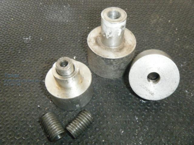 The one on the left is used the most, it has three 'inserts' for different tap shaft diameters. The one on the right is similar but just for one size shaft. The one at the back is for a bigger shaft still. The trick is to hold the base firmly onto the surface being tapped as the thread is started. It will be perfectly at right angles to the surface every time. Klaus |
||||
renewableMark Guru Joined: 09/12/2017 Location: AustraliaPosts: 1678 |
You know what, if I saw on ebay a tap with a matched alignment collar I'd buy that, you should think about it. Edit I don't want to give you a big head though. Cheers Caveman Mark Off grid eastern Melb |
||||
| Tinker Guru Joined: 07/11/2007 Location: AustraliaPosts: 1904 |
Thanks Gary, I just fired up this inverter for the first time and it ran fine. Turning it off and on several times no problem. Perhaps its because I have a biggish capacitor at the 12V line of the control board. Wiseguy, This power supply is *not* isolated either. This does not bother me with the ~55V input. Actually I do use the common negative as a power return line, the gate drive must reference to a common ground at the low side. Klaus |
||||
| Tinker Guru Joined: 07/11/2007 Location: AustraliaPosts: 1904 |
I did  , many many years ago, well before anybody even heard of 'Ebay' , many many years ago, well before anybody even heard of 'Ebay'  Klaus |
||||
Madness Guru Joined: 08/10/2011 Location: AustraliaPosts: 2498 |
Isolated DC to DC power supplies are very expensive and you certainly would not bother with them unless it was absolutely necessary. There are only 10 types of people in the world: those who understand binary, and those who don't. |
||||
| Tinker Guru Joined: 07/11/2007 Location: AustraliaPosts: 1904 |
So my inverter was powered up for the first time today  . It ran as expected and the standby power was 11 Watts. . It ran as expected and the standby power was 11 Watts.  To continue this build; the brain of this thing is the EG1810 chip, a 32 pin surface mount device that requires soldering onto a small PCB carrier board so it becomes plugable. Here is how I do it. Beside the little PCB, which comes in a multiple, break off a piece as required format, a single in line row of header pins and sockets for these is also required. The header pins/sockets come in a strip of 40. 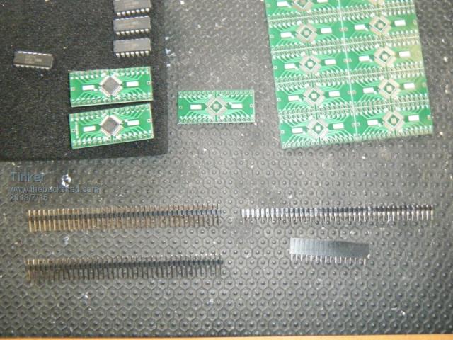 The pins are easy enough to cut to 16 with a Stanley knife, cutting between the pins. The sockets need to be cut at #17 to get 16. Not possible to cut these between the contacts. BTW, the sockets I use must be the taller ones, like the 16 pin one at lower right. The 40 pin version, shown at upper right, is too low to raise the board over the crystal & 2 capacitors located inside the socket rows and also to accommodate the long pins fully. Soldering the SMD chip is a bit fiddly but easy enough. 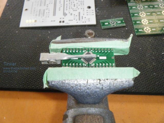 I use a little clamp to hold the chip firmly in place, making sure the pin 1 dot aligns with the pin 1 PCB pad. Carefully pushing the chip about with a pointed tool does the trick. Soldering is by solder paste only, no solder wire. And a very fine (0.8mm) soldering iron tip is required. The solder paste comes in a little tube with a tiny nozzle which works well when new. only a very small amount at the end of the chip 'leg' is required. When this paste has been lying on the shelf for a while the stuff goes less runny, at least mine did. So I use a 1mm jewelers screwdriver to transfer the small amount to the chip leg, that works just as well. Having my elbows firmly on the bench top, holding the soldering iron steady with both hands while peering through the magnifying glass, the tip it brought in contact with one 'leg' end. The paste will instantly flow into a shiny solder joint if this is done right. Next solder a 'leg' diagonally opposite, this locks the chip in place and the clamp can be removed. 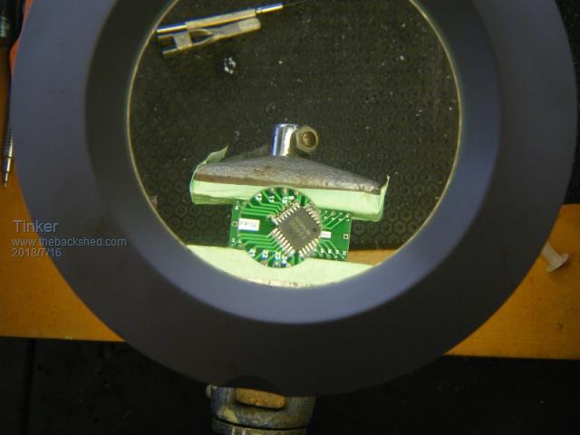 After soldering all legs the flux needs to be carefully removed. I use PCB cleaner spray with the long tube nozzle and an old tooth brush. Isopropyl alcohol does not works so well for this in my experience. Then the lot has to be very carefully inspected under a good magnifying glass to check for solder bridges, solder globules between the 'legs' and resin that could hide those. To solder on the 16 pin SIL headers I find it easiest to do this on the control board before anything else has been soldered onto it. The board is just used to keep the two pin rows steady and square while the shorter pin ends are soldered to the little PCB carrier. 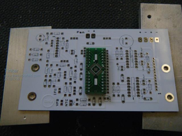 Its a good idea to make several of these complete plug in EG1810's. The chip is not bullet proof and its good to have an instant spare or two. One has to order 10 boards and 10 chips anyway. To be continued, next main the PCB. Klaus |
||||
| Warpspeed Guru Joined: 09/08/2007 Location: AustraliaPosts: 4406 |
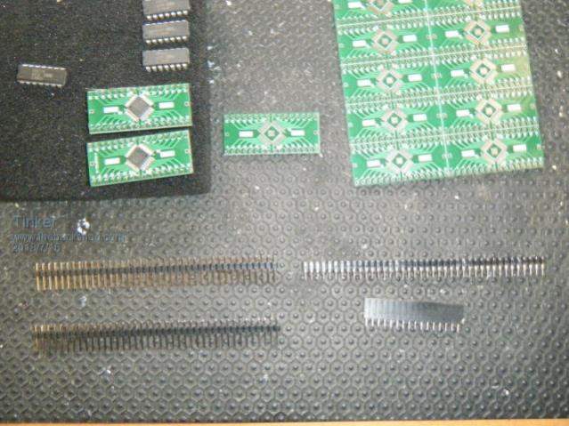 Its probably perfectly obvious, but when soldering the header pins and sockets to the PCBs, especially the longer variety, its important that the two rows of pins are straight and parallel so they will mate correctly. The easy way is to plug the pins and sockets together, and then plug both rows into two circuit boards. That holds everything perfectly in line while soldering. That tap guide "thingy" is something I have never seen before, and for years I have been tapping crooked holes. Thank you Klaus !! Its amazing though, how the simple tricks of the trade that are perfectly obvious once seen, may not be that obvious after all. Cheers, ĀTony. |
||||
| Tinker Guru Joined: 07/11/2007 Location: AustraliaPosts: 1904 |
Today's testing had the little inverter doing 2700w with just 4 Mosfets. No problems at all. I have now fitted all 12 Mosfets and am waiting for a really sunny day so I can test just how far I can push that thing  . .Now to continue with the build description. Looking at the power board schematic below it is obvious (to me at least) that there are two *identical* circuits to it. So it made sense (to me) to have the parts located on two smaller, identical, PCB's. Since 2 oz PCB'a are expensive anyway and the larger they are the more $$ they cost its a win win. As there is a minimum order quantity from the board makers, having two instead of one board is no problem. Also, I found it much easier to lay out the smaller board on the laptop screen. A downside might be one cannot use that ribbon cable for the gate drive signals but for me its not a great idea anyway. I much prefer individual wired gate drives, no long tracks on a large PCB. 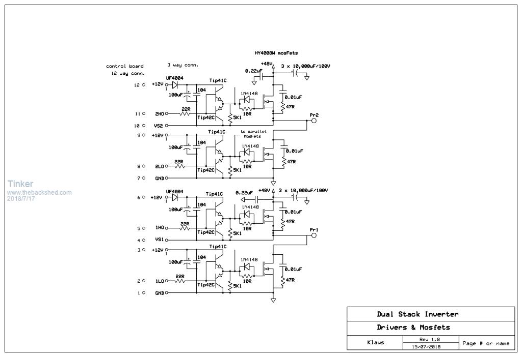 So this is what my power boards look like, shown top & bottom side of one board. As mentioned, there are two of those boards used. Components are soldered onto both sides of the board. I used extra solder lugs at the capacitor terminals for beefing up that area. The power track vias have been filled by soldering 1mm tinned wire links in to raise the current capacity of the vias. The alternative was to have dozens of plated through holes for which there was not enough room. 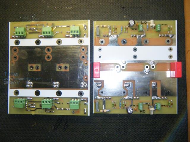 Looking at that picture you will notice something odd with the solder resist screen. I fess up, I goofed there  . Somehow the Gerber files ended up the negative image of what I wanted . Somehow the Gerber files ended up the negative image of what I wanted  . The board makers tell me the resist layer will not come off without damaging the tin plating. . The board makers tell me the resist layer will not come off without damaging the tin plating.But the board is perfectly usable, I just cut small thin washers from solder lugs and placed them where the screws pass through the board. These are high current areas, I made sure I got tin plated copper lugs - they also sell them in brass, tin plated, which look exactly the same. The component silk screen is a bit meager, the free PCB layout program (Design Spark) does have an extensive library but its linked to the foot print of the part manufacturer. So the pad sizes, spacings, etc. are a bit too crammed for a board with relatively few parts on it. I prefer to have bigger pads and wider spacing that can stand up to de-soldering... So, no "painting by numbers" here. I think it is better having to follow the schematic & tracks to locate which part goes where, this should help a lot for understanding how everything connects together. On this board there are screw terminals used for the Mosfets as well as for the totem pole drivers. 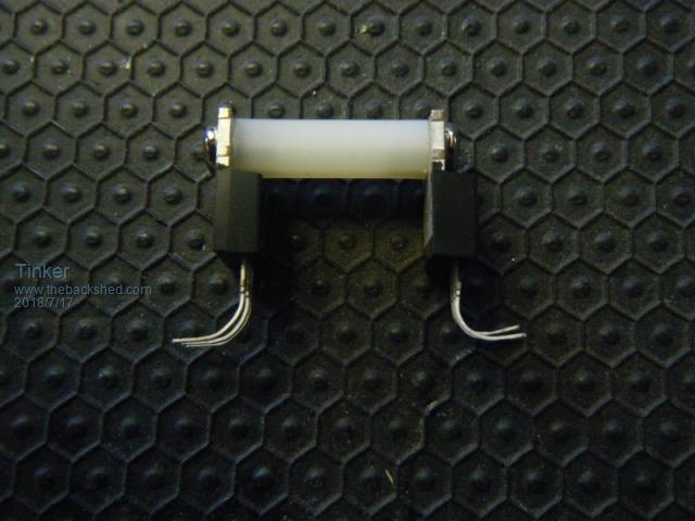 Note how the totem pole transistors are oriented and held together by a 25mm plastic spacer. The latter is to prevent constant bending of the 'legs' when the board is handled. The legs are bent to insert into the terminals, they were oriented this way as it made the resulting PCB track layout much easier. There is a 3 way pin header located between the totem pole drivers, its where the gate drive connector goes. The boards are numbered 1 & 2. Each has a high and a low side. So 1LO means low side board one. 1HO means high side of board one. I marked the plugs accordingly since each gate lead has the same length wires. 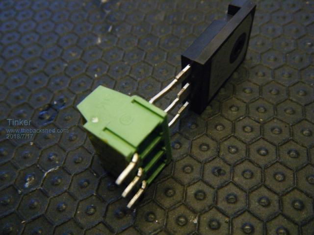 The Mosfets connect into vertical terminal blocks. They provide excellent access to remove or insert the part. However, it can be seen that the back of the terminal is open, so I located them a little further from the heat sink to prevent flashover at magic smoke events. There is a 25 x 6 mm alu strip spacer to compensate for that. I also stuck a strip of klapton tape to the terminal underside (against the PCB) for the same reason of flashover minimising. Prevention is easier than cleaning up the black charred mess. However this has not been tested yet, so far the inverter behaves admirably  . .Since the power PCB directly screws onto the heatsinks, the mosfet legs do no heavy heat sink supporting duty at all. One or even all at once can be replaced quickly and everything else stays in place. Perfect for the experimenter  . .A hint about soldering components. I always start with inserting the lowest height parts first. This is so when the board is turned over for soldering these they all remain pushed against the board. I don't use those PCB holding contraptions. 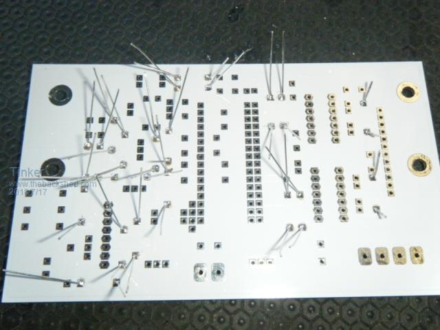 I only slightly splay the 'legs' so the part remains on the board when turning it over for soldering. For a good mechanical fixing the legs should be turned hard over and cut at the pad edge. Very essential if the board is subjected to vibrations. But for me, where on occasion a part has to be unsoldered, such a method would make that unsoldering difficult. So I leave the leg intact for soldering. This also prevents semiconductors from getting too hot if one is a bit slow with that soldering. The legs are cut after soldering, this also assists when checking if each leg is indeed soldered since one has to look at it to place the side cutter. When soldering multiple pin parts, like DIL sockets, I always solder a corner pin on each row, at opposite ends, first. Then I turn the board over and check if the socket is indeed flat against the board. If it is not, its easy to apply the soldering iron to the pin soldered while pushing the socket in by finger to correct. Quite impossible to do if many pins were soldered on each row. Here is the completed control board. 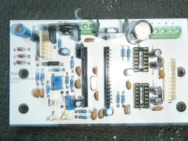 I will describe in detail how I test this later. It may be noted there are extra pin headers next to pin 1 of the EG1810 carrier. They are for dead time selection my means of placing these 2 pin shorting plugs over the selected pins. My board can accommodate two different row spacing EG1810 carrier boards, I think the one madness did is uses the wider carrier board. Those blue 25 turn trim pots is what I prefer for this project. They allow a very fine adjustment and have a very small footprint on the board. They're sealed too. This board is held in place on the power board by brackets made from 3mm alu angle. One of the brackets conveys the battery voltage to the board for the low battery sensing. The 12 pin header on the right is for the gate drives. The 8 pin header on the left top is for the switch box containing the on/off SW, reset PB, LED's. The two pin headers are for VFB, IFB, TFB. Next, setting up and testing. To be continued. Klaus |
||||
Madness Guru Joined: 08/10/2011 Location: AustraliaPosts: 2498 |
Klaus if you don't have it already Gerbv lets you view the Gerber files to confirm they are correct before sending them off. JLC PCB are very similar to PCBWay, I have heard JLC is as good but have not tried them myself. What is really nice is when you upload your files for a quote it creates an image of the PCB so you can see exactly what you are going to get. There are only 10 types of people in the world: those who understand binary, and those who don't. |
||||
| Tinker Guru Joined: 07/11/2007 Location: AustraliaPosts: 1904 |
Thanks Gary. I think I do have that gerbv program but was obviously too lazy or forgot (more likely  ) to use it. ) to use it.I will look into that JLC PCB next time I do a board. I just hope the 'learning curve' is not as steep. There are a few very annoying (to me) features with that free design spark program anyway. At first it went right through all my .pcb files on the computer, even if they were done in a completely different program (Express PCB), and renamed them as design spark.pcb. This, of course makes them unreadable for the original program as well as for design spark. I have found a way around that but its bothersome. Klaus |
||||
Madness Guru Joined: 08/10/2011 Location: AustraliaPosts: 2498 |
I found it a must do step to use Gerbv, you no doubt have come to that conclusion also. JLC is easy just try one of your existing files to get a quote you will see what I mean. As for Designspark it probably asked if you wanted to change the files or at least it should have. There are other options but it is only the only free software that I know of that will allow doing larger PCBs. There are only 10 types of people in the world: those who understand binary, and those who don't. |
||||
| Tinker Guru Joined: 07/11/2007 Location: AustraliaPosts: 1904 |
There was a short sunny break today to allow full power testing of inverter #4. This was the result: 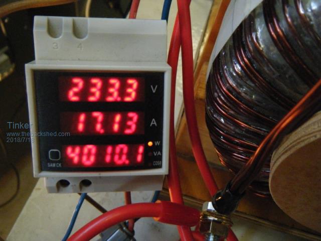 It ran as expected, in fact better than that. Of course, using a 2.5Kw rated toroid with the original 320v winding and having only a 12.5mm sq primary was asking a bit much from that to handle the 97 Amps coming from the battery.  . .As a result it took not long for the primary wires to register 90 degrees on my infrared thermometer. I turned the power down then. But the heatsinks with the 12 HY4008's installed got barely lukewarm. So the thing would easily handle a twin stack Aerosharp type core toroid with just 12 Mosfets. Me thinks now that using 24 mosfets in my other two inverters was a bit of an overkill. Besides, it is a lot easier to match the on resistance of the paralleled Mosfets in just batches of three. Mine were matched to be within 0.02 milli Ohms. To continue my build description, this is how the mosfets are mounted on the vertical entry terminal blocks. 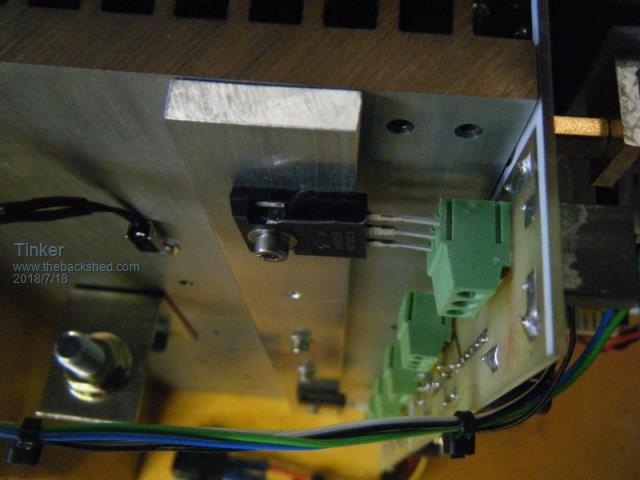 Good clearance for the 'legs' but they are left at almost their full original length to get the mounting screw in between heatsink fins. I suppose one could argue this gives more cooling area for the 'legs'. Now a few pictures of how the lot fits together. 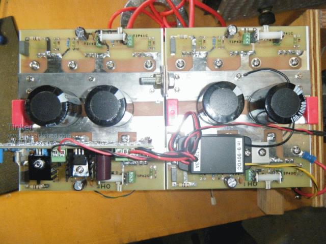 Looking from the top of the power boards we see how the control board mounts on spacers on the left. The board must be located on the long heat sink side as one spacer conducts the +battery voltage to the board for sensing. On the right is that little DC/DC converter mentioned on an earlier page. One of the two common links between the boards are the two -battery copper busbars with the connection between the boards for current sharing. The positive common link is, of course, the large heat sink. 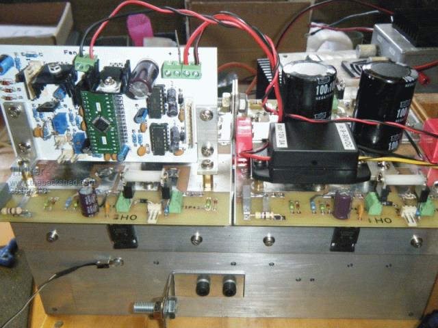 Here we look side on to the control board and see how it is mounted. This comes off very easy, just unplug the headers & power wires and undo 2 M4 screws to the brass spacers. The spacers are a M4, 15mm long, male/female thread version. 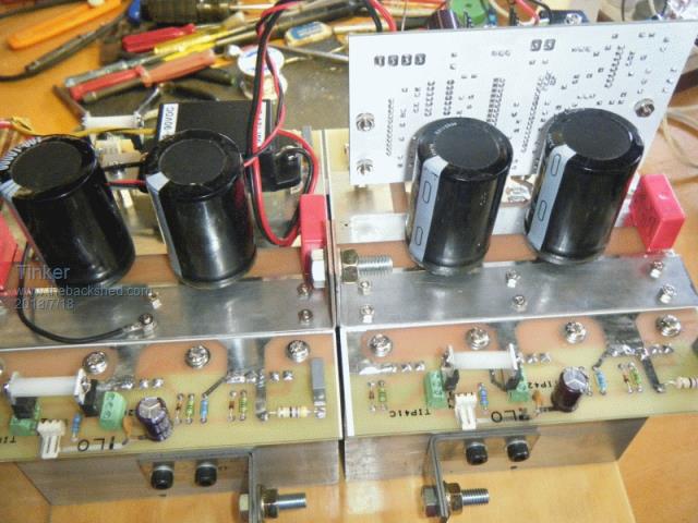 This is a view from the other side of the control board. Mark, if you look closely you can see the advantage of having screw terminal capacitors  . The busbar can fit partially under them, thus saving board area. More area = more $. . The busbar can fit partially under them, thus saving board area. More area = more $.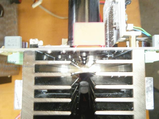 Now a picture looking at the upper end of the heatsinks. This shows how the extended heatsink base width allows above first fin clearance for the screw heads on the PCB underside. Sorry about the poor quality pic. 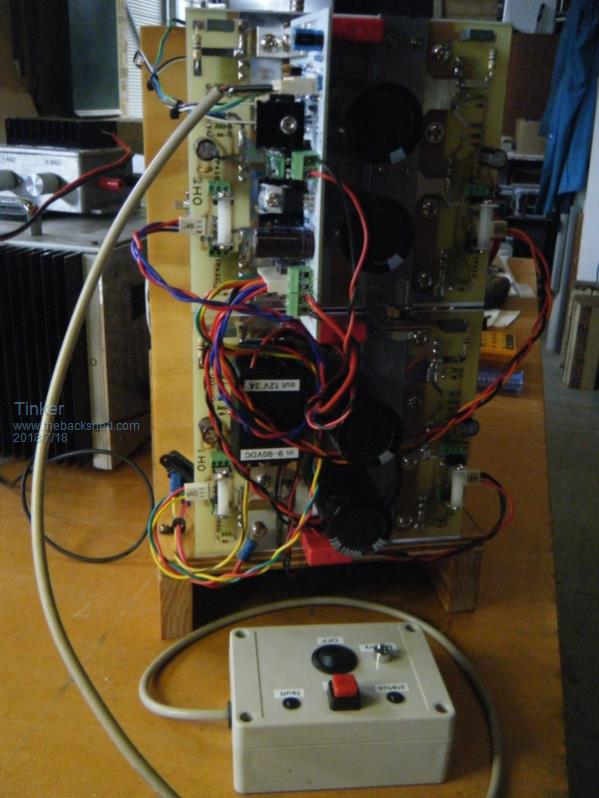 Next an end on view showing the gate drive wiring. As mentioned, they are all the same length and I plaited them to bundle the 3 wires neatly. Last picture is of my switch box which plugs into the 8 pin header. This proved very useful for inverter #2 & #3 during testing. It could be used as a permanent control for this inverter, it does all that's required to run it. 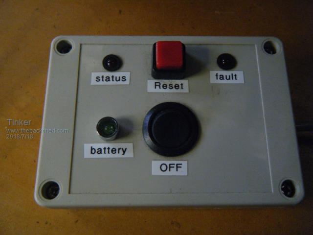 To be continued. The next part describes hoe I set up and then tested this inverter to run successfully first time. Klaus |
||||
| Warpspeed Guru Joined: 09/08/2007 Location: AustraliaPosts: 4406 |
Very nice indeed Klaus. What are you using for a choke ? Cheers, ĀTony. |
||||
| The Back Shed's forum code is written, and hosted, in Australia. | © JAQ Software 2026 |