
|

|
Forum Index : Electronics : A newbie ozinverter build
| Author | Message | ||||
| tinyt Guru Joined: 12/11/2017 Location: United StatesPosts: 556 |
Hi Klaus, Thanks for your technical and safety advice. I quickly looked at the forum post and I envy your electro-mechanical skills. Will go thru it slowly. I was able to buy from ebay four 150x69x37mm heatsinks. Free but slow shipping, but I am not in a hurry. 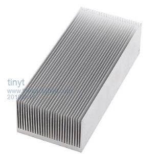 I hope it is adequate. Dense fins - efficient heat dissipator and dust catcher. I don't know how thick the base is, I still have to figure out how to bolt it edge-wise thru the PCB. I might still want to experiment on the flimsy angle bar sinks to find out how much load it can tolerate. The 2.2 KVA toroid I ordered from ebay came. 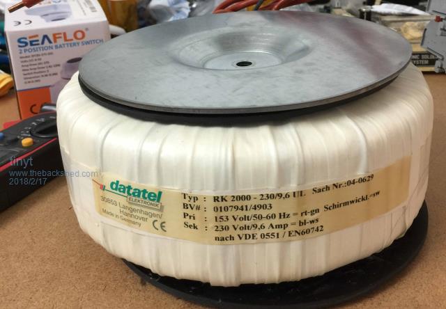 It might be light for others but it is already too heavy for me. I guess I need to take idle power measurements, turns/volt, etc. before I hack it. If the secondary is wound first, I will attempt to split the winding in two to get double 115 vac sections without unwinding it to save on labor. I hope my arthritic fingers can still do the unwinding and re-winding. |
||||
Madness Guru Joined: 08/10/2011 Location: AustraliaPosts: 2498 |
Mounting the heat sinks is easy, just drill and tap them with M3. even the 12 FET version easily supports the heatsink, I just put a perspex sheet on tap to stabilize it and it is solid. There are only 10 types of people in the world: those who understand binary, and those who don't. |
||||
| Clockmanfr Guru Joined: 23/10/2015 Location: FrancePosts: 437 |
You have probably seen these before. This is the most used method for heatsink mounting and compactness, but sufficient clearance distances and spacing for ease of construction and longevity. The heat sink gives rigidity to the double copper thickness, and double sided PCB Power board as its nearly A4 size. 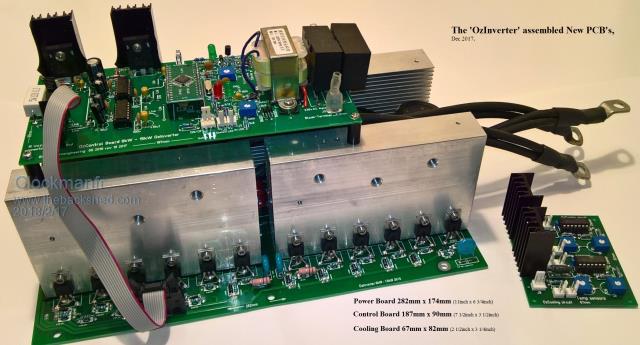 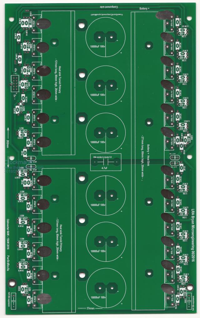 Everything is possible, just give me time. 3 HughP's 3.7m Wind T's (14 years). 5kW PV on 3 Trackers, (10 yrs). 21kW PV AC coupled SH GTI's. OzInverter created Grid. 1300ah 48v. |
||||
| tinyt Guru Joined: 12/11/2017 Location: United StatesPosts: 556 |
Thanks Madness and Clockmanfr. Those pictures are great and clarified a lot of things for me. I assume that the tapped holes (4 for the long heatsink, and 2 for each shorter heatsink) for PCB mounting are on the fin at the edge of the heatsink. The fins of the heatsink in the picture look to be thicker and can be tapped to take the screw threads, but the ones I ordered look very thin. I don't know how many threads it will hold. Maybe I have to carefully drill and tap thru several fins to make a solid mounting. Also I thought that the heatsink particularly the long one has no insulator at the mounting surface and just relied on the soldermask. Thanks for telling me to use perspex (acrylic sheet?) or rubber strip. One question. The 3 legs of the mosfets are in-line when received, but the picture shows the outer legs to be bent forward/outward. Is it to allow more copper to surround the source and drain legs of the mosfets? |
||||
Madness Guru Joined: 08/10/2011 Location: AustraliaPosts: 2498 |
The 3P package of the HY4008 MOSFETs is designed to have the pins in a straight line, clockmans boards are designed for TO220 package MOSFETs as shown in the heatsink photos. You can bend the legs of HY4008's to make them fit but if you designing your own PCB you are much better off having the legs all in a straight line. They will then drop straight in and keep the legs as short as possible as they are designed to be used. I was referring to using perspex on top of the heatsinks to keep them in a fixed position, rubber is suitable. There are only 10 types of people in the world: those who understand binary, and those who don't. |
||||
| tinyt Guru Joined: 12/11/2017 Location: United StatesPosts: 556 |
Got it on the Perspex. Clockmanfr's 'exploded' picture shows the black rubber strip placed near the heatsink mating surface for the PCB. So, two different things I think. On the mosfets, even the 16 HY4008 oztules gerber shows them spread out. But per your advice, I will layout the PCB with them in a straight line. Thanks. |
||||
Madness Guru Joined: 08/10/2011 Location: AustraliaPosts: 2498 |
Here is one of my PCBs you can see the perspex on top of the heatsink and MOSFETs. The bottom image is an earlier version, I have now increased the area not covered by the solder mask. So there is now a larger triangular area of solder around each leg to spread out the current. I have run this design at 8KW for 30 minutes with no problem. The PCB is 300 X 300 MM so that will give an idea of the size of the heatsinks, they probably don't need to be that big but what you see is the largest size that fits in the case. 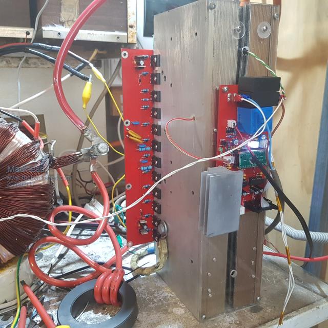 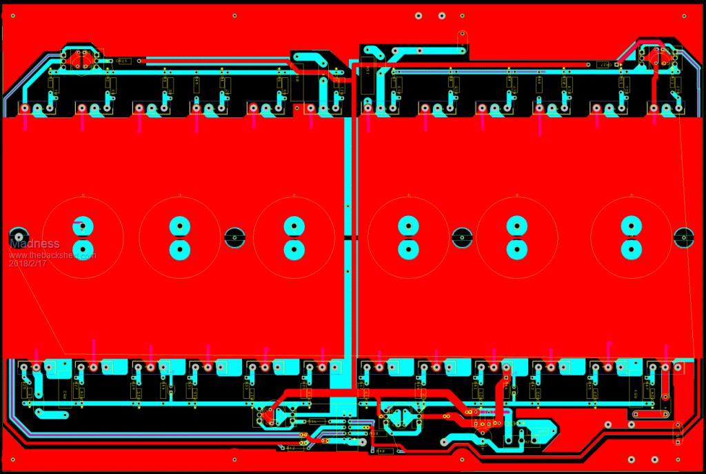 There are only 10 types of people in the world: those who understand binary, and those who don't. |
||||
| tinyt Guru Joined: 12/11/2017 Location: United StatesPosts: 556 |
Hi Madness, Those heatsinks are huge. Without seeing your picture, I would normally bolt the heatsink to the PCB and mount the PCB/heatsink assembly by the mounting holes of the PCB. But your picture shows a different way. Attach the PCB to the heatsinks via the mosfets and their legs, no need for bolt holes on the PCB. That is how I interpret the picture. If the perspex is thick enough and made wider, and mounting holes are drilled at their corners then the entire assembly can be mounted to the cabinet via the perspex mounting holes. The screws to attach the perspex to the heatsink can be flat head nylon screws to isolate the heatsinks from the metal cabinet. Maybe metal flat heat screws will also work if their heads are covered with kapton or vinyl tapes. I like it. Your toroid shows multiple strands for the primary (x in hand - is that how you call it?). That is also how I will do it on my toroid as my tiny hands will not be able to work the huge cables I usually see. So, it is OK to use no gap toroid for the series inductor? Looks like you have discrete complementary transistors/mosfets for the gate drive of each group of HY4008. Will they be needed for a group of 5? Sorry for all the questions. Thanks for the picture. |
||||
Madness Guru Joined: 08/10/2011 Location: AustraliaPosts: 2498 |
That toroid is something I threw together for testing only, welding cable with the only the inner silcon insulation is very soft and flexible, it is much easier to wind. I am not with you regarding the perspex, I mount the PCB via the holes in the PCB, then all the connections need to be made, that would be impossible with a full width perspex and also leave the control board exposed. There are only 10 types of people in the world: those who understand binary, and those who don't. |
||||
| Clockmanfr Guru Joined: 23/10/2015 Location: FrancePosts: 437 |
tinyt, The FET's legs are like the ones shown for the 4110's but the Power board will also take the larger FET's like the 4008 without any modifications. Just slightly bend the legs so the FET sits up flat against the heatsink. See photo, 4008 FET just dry positioned for illustration purposes. Originally I examined the available FET packages and allowed for several FET sizes. For me its all about designing a PCB Power Board that will take a variety of differing size and type of components without the reliance on one particular size or brand. In the very beginning of this OzInverter project we did not want to be subject to specialised specific components. 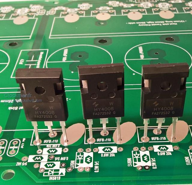 Yes, drill through a few of the heatsink fins and tap for the thread, I tap about 20mm in depth as a minimum. But watch the swarf from the drilling as it needs to be thoroughly removed, or else there could be a disaster if the bits of aluminium later drop on to the board.! Everything is possible, just give me time. 3 HughP's 3.7m Wind T's (14 years). 5kW PV on 3 Trackers, (10 yrs). 21kW PV AC coupled SH GTI's. OzInverter created Grid. 1300ah 48v. |
||||
| tinyt Guru Joined: 12/11/2017 Location: United StatesPosts: 556 |
Hi Madness, In your gerber picture, are the PCB mounting holes for the heat sink the four black holes that are in line with the large capacitors, or closer to the mosfets but only cannot be seen in the picture. Hi Clockmanfr, Now I understand. I agree the more universal the design is, the better. Are the oval solder mask to allow more solder and higher current flow for the source leg of the mosfets? Thanks for the reminder to remove debris and deburr after machining operation on the aluminum. |
||||
Madness Guru Joined: 08/10/2011 Location: AustraliaPosts: 2498 |
There are no heatsink mounting holes in my PCB they are not needed. There are only 10 types of people in the world: those who understand binary, and those who don't. |
||||
| Tinker Guru Joined: 07/11/2007 Location: AustraliaPosts: 1904 |
Now that really surprises me. I though you would take advantage of the *huge* current carrying capacity of these aluminium heat sinks and use this feature to unload some the 2oz PCB tracks. This also frees the center Mosfet leg from heavy current duty. The idea certainly works on my PCB. Klaus |
||||
Madness Guru Joined: 08/10/2011 Location: AustraliaPosts: 2498 |
The heatsinks in my inverter do carry current and do exactly as you described, it was you, Klaus, telling me how you did not like my "hot heatsinks" and that you did not like that idea. You also went on to tell me how you would not build an inverter that way after I suggested it had it's advantages. It's in your inverter build thread if you want to go looking for it! What I said is "there are no heatsink mounting holes on the PCB" MOUNTING being the operative word, nothing electrical about it. There are only 10 types of people in the world: those who understand binary, and those who don't. |
||||
| Tinker Guru Joined: 07/11/2007 Location: AustraliaPosts: 1904 |
Yes Gary, I was on a learning curve too back then. I originally wanted an external heat sink, like the original Aerosharp had. That meant it could not have any other than an earth connection for safety reasons. Anyway, the idea did not work in practice. I admit I was barking up the wrong tree with that idea as the inverter started to work once I used 3 separate 'electrified' internal heat sinks and a fan blowing at them. We may have a mis understanding about the heatsink - PCB mounting method. Here is how mine works: Power (+V, primaries) connection on heat sink. Now the primary connections require contact to PCB tracks, I did that by bolting the heat sink edge directly to the PCB track. Works a treat and removes the mechanical heat sink fastening from the Mosfet mounting screws. I also use 3 way terminals for each mosfet. This lets me remove each or all mosfets without having a loose heatsink to deal with. An advantage in my PCB/ heatsink assembly. If you wish, I could see if a screen grab of the PCB helps with digesting this. Klaus |
||||
Madness Guru Joined: 08/10/2011 Location: AustraliaPosts: 2498 |
Okay that is slightly different, my heatsinks don't make contact with the pcb. The MOSFETs are screwed to bare metal on the heatsinks. I have not seen any reason to change this, the MOSFETs are as close as possible to the PCB with large solder pads to spread the current up the MOSFET leg and across the PCB. Works for me, runs at 8KW for at least 30 minutes. I see no good reason to change it anyway. If I need to take it apart it only takes 2 minutes to undo all 24 screws with the electric screwdriver. I have no plans to change the inverter in the foreseeable future, currently I am working on networking my GTI's and to limit their output so I don't push too much power back through the inverter. There are only 10 types of people in the world: those who understand binary, and those who don't. |
||||
| Clockmanfr Guru Joined: 23/10/2015 Location: FrancePosts: 437 |
Yes the oval shape of the solder pads allows a little more solder to be added around the FET legs to spreading the loading onto the copper pinch areas. 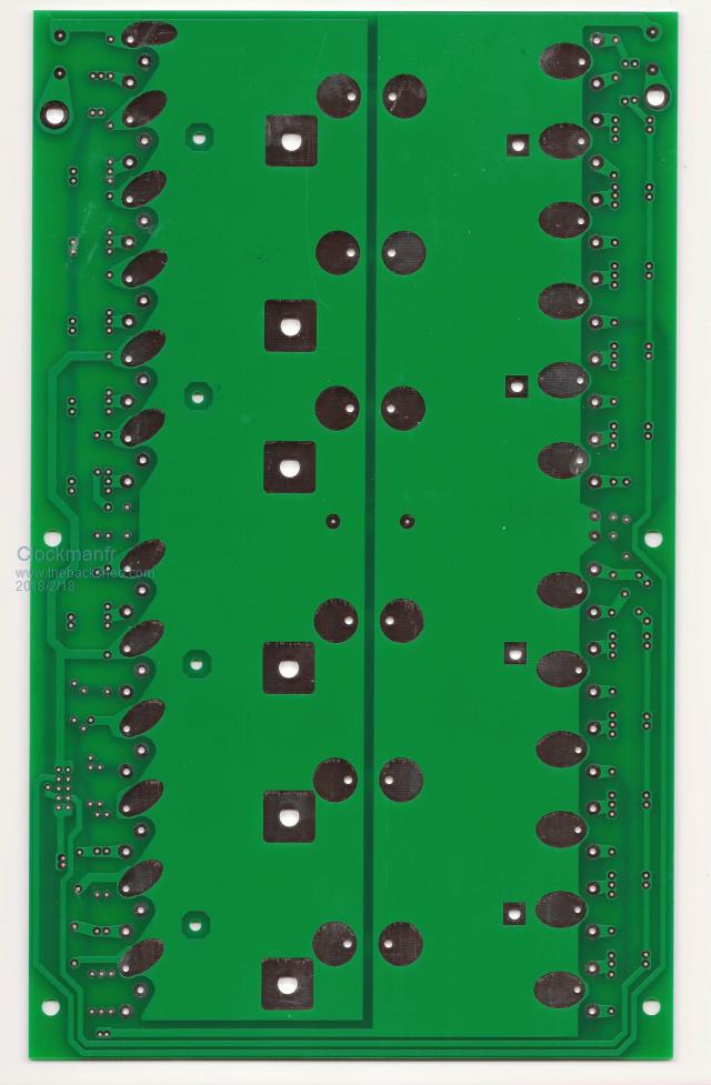 Here is a photo of the underside of the OzInverter board, as you can see Ovals on those load pinch points. Also in the Photo the 4 holes for the 48v + battery positive heat sink allow direct connection between the heatsink and the main copper on the under side, as in this photo. I trust this helps? Everything is possible, just give me time. 3 HughP's 3.7m Wind T's (14 years). 5kW PV on 3 Trackers, (10 yrs). 21kW PV AC coupled SH GTI's. OzInverter created Grid. 1300ah 48v. |
||||
| Tinker Guru Joined: 07/11/2007 Location: AustraliaPosts: 1904 |
I did not suggest you change anything, if it works let it do so. Just pointing out a different way which removes high currents from one of the Mosfet legs - a weak point of them IMO. Klaus |
||||
| tinyt Guru Joined: 12/11/2017 Location: United StatesPosts: 556 |
Yes, thank you very much. I am still waiting for the heatsink before I do the gerbers. Also, doing some schematic changes. I received an egs002 board today and for now doing stand alone test of the pwm signals. I have confirmed the 'scope signals at the TESTx points. Doing more testing. |
||||
| tinyt Guru Joined: 12/11/2017 Location: United StatesPosts: 556 |
Had some time to work on this. The schematic has now evolved, it even has the kitchen sink.  This could become my lifetime project.  2018-02-26_083756_Experimental_Inverter.pdf |
||||
| The Back Shed's forum code is written, and hosted, in Australia. | © JAQ Software 2026 |