
|

|
Forum Index : Electronics : building an Inverter from scratch
| Author | Message | ||||
| Warpspeed Guru Joined: 09/08/2007 Location: AustraliaPosts: 4406 |
Inverters are possibly the worst possible thing to design and test, especially if they are to be sold commercially to idiots. The reason being you simply have no control over what some fool will plug into it. If we only had to deal with resistive loads within some limited range it would be easy, but its far worse than that. Even doing it for just ourselves its far from easy and fraught with difficulties. PWM adds another extra dimension of complexity. The old push pull low frequency square wave inverters were much easier to get going, and far more robust. I have had more than my share of grief with PWM inverters when I was doing this for a living. I hate the damned things, which is why I decided to completely avoid PWM in my own home built inverter. There is no simple easy solution to all this unfortunately. All you can do is be scrupulously careful and pray a lot. Start out at very low voltage and current, and gradually work it up, monitoring absolutely everything as you do. If it goes bang, there will always be be a reason why. You have to be a Sherlock Holmes and examine all the clues that lead up to the "event". Cheers, �Tony. |
||||
| Tinker Guru Joined: 07/11/2007 Location: AustraliaPosts: 1904 |
Hi madness. I think I'm on the trail of something with our inverter problems. Perhaps you could check along the same lines and between us we *will* solve this frustrating conundrum. Anyway, I just perused (again) the application notes for the EG1810. On page 12 under "AC Output Voltage Feedback" I found two things that are different on my PCB. The first "A filter inductor needs to connect to SPWM output port" I have not done that. Its not on the little EGS002 boards either and oztules also does not have them on the PCB screenshots he posted a while ago. Do you think that's worthwhile to investigate? If so, what size inductor? I think I'll get some of those little ones that look like a resistor and try them. The second, and IMO more important, difference: "voltage feedback is through measuring the AC voltage output of inverter." Here I just reverse engineered what oztules had on his PCB which obviously works. He rectified the output of the little 12V transformer. But then its no longer AC that gets sampled! I think the 8010 is looking for an AC waveform on its VFB (pin 13) input. Presenting the DC ripple of rectified AC 'might' work but it also might not. I certainly will now go and try that. If I am right then I will post an altered schematic here later and I'm sorry for not picking this up sooner. Now lets see what else I can find, I'm almost convinced something is wrong with the signals driving the gates rather than with the Mosfets themselves. Klaus |
||||
| Warpspeed Guru Joined: 09/08/2007 Location: AustraliaPosts: 4406 |
Just playing devil's advocate here, but...... One evil thought has occurred to me. These EG1810 boards, are they all identical and from the exact same supplier ? Can we be sure ? The Chinese love to copy things, and there may be subtle differences in the software between different sources or even batches of these boards, especially if there are non genuine copies out there. Any product that is popular and sells well gets copied by the Chinese. It seems very strange to me that some people have no problems and others seem to be cursed. Cheers, �Tony. |
||||
Madness Guru Joined: 08/10/2011 Location: AustraliaPosts: 2498 |
Hi Klaus, Just looked at the circuit in the EG8010 data sheet and I can't see the inductor you mention in the VFB circuit, as far as I know it is DC and needs 3 volts at the chip. In the EG8101 data sheet on page 12, I can see a circuit there with the inductor which is the choke that we are using, sorry if I am missing something here. For testing, I have connected the 12V supply to the diodes on the Oztules control board. This allows me to have the control board running on it's own. I am using this to test the Gate drive boards I am making with the TC4452 chips. The PCB's are just 22 X 26 MM, the chips have just arrived. Tomorrow I have time to work on it, fingers crossed I will have a positive outcome. Warp I know the EG8010 chips I am using came from the same supplier as Oztules so a good chance they are the same. I doubt they are the problem though as I get good results with a limited number of FETs. But until I get it right I do not know what they problem is. Hopefully, the TC4452's with more grunt will make it all work the way it is supposed to. There are only 10 types of people in the world: those who understand binary, and those who don't. |
||||
| Tinker Guru Joined: 07/11/2007 Location: AustraliaPosts: 1904 |
Hi Gary, The manual is not worded very clear with regard to the inductor. As I read it there should be a conductor at each of the SPWM out (pins 27-30) of the 8010. But I might be wrong. The other thing, look at the circuit schematic on the EGS002 datasheet (you'll need a magnifying glass). The VFB (pin 13) samples the **AC** of the transformer output. We put a little 12V transformer there to isolate this sampling from the high voltage side. But its still AC that is being sampled, there are no rectifying diodes used on that circuit, neither are there any in figure 8.1a (page 12 of EG1810 datasheet). So, why did oztules rectify this feedback voltage? I have just removed this rectifier from my transformer output and the inputs to the IR2110's still look good. I'll get some more parts tomorrow and continue my testing. Klaus |
||||
Madness Guru Joined: 08/10/2011 Location: AustraliaPosts: 2498 |
On page 10 we have diodes, there is no transformer but we know Oztules added it for a good reason that caused him problems when his batteries got wet. But what matters is diodes = DC. 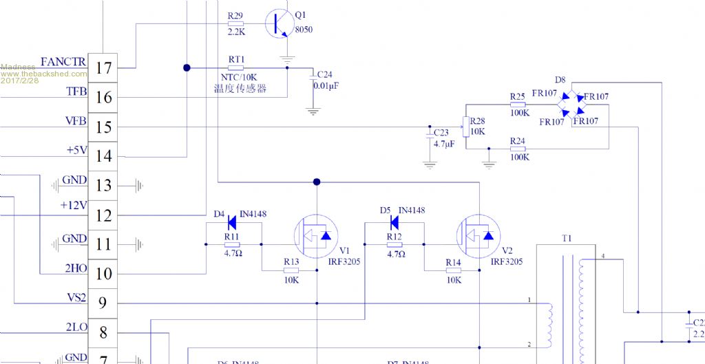 This version is low voltage with a transformer same as we are building. The Chinese manuals are not perfect either so you are right to doubt everything. There are only 10 types of people in the world: those who understand binary, and those who don't. |
||||
| Tinker Guru Joined: 07/11/2007 Location: AustraliaPosts: 1904 |
Gary, I cannot find that page. Any chance of the correct url? The manual I look at (EGS002) only has 6 pages. The one for the EG8010 does not have the schematic above. It must work with AC fed into the VFB input as well or the schematics I can see are all wrong. Klaus |
||||
Madness Guru Joined: 08/10/2011 Location: AustraliaPosts: 2498 |
The EG8010 Datasheet is here this from EGMicro. This is the version of the documentation that I took the image from. If you have a look at the EGMicro download page you will find other incarnations of the circuit using different driver chips, no doubt this will keep you occupied for a few hours. If you can read Chinese there is a version 2.2 of the manual, the circuits, fortunately, are in english. There are only 10 types of people in the world: those who understand binary, and those who don't. |
||||
oztules Guru Joined: 26/07/2007 Location: AustraliaPosts: 1686 |
Klaus, I have not been following this very closely lately. Right, the transformer on the VFB is only necessary if you have an earthed system. Look at the circuit provided by madness... it is obvious that any earthing regime will short out one side of the voltage splitter... and your unit will run between 240 and 120 v depending on the impedance to ground of the battery bank. A isolating transformer fixes this... otherwise an opto would do the same thing. The VFB uses DC to control the AC output. The big inductor is only there to damp the very high frequency wave front of the switch. Thats why it is so small in uh.... it is looking to damp up in the 100mhz range, not the 20khz range. The rapid rise in current from zero to maybe 100 amps or more in nano seconds makes the DC look like a ac wave front... bit like lightning I guess. This burns up power showing up as idle current losses. These aren't recoverable without the inductor.... thats all it is for. This inductor can effect the wave form, and maybe warp can explain how or why... but I suspect it is only able to do that because the driver is a bit weak. I think that the damping loads the fet channel up more, and this will exhibit as a magnetic field on the channel side of the oxide gate... 100 or more amps of current must have a magnetic field of some size. Magnetic field can effect the charged electrons on the gate side of the oxide, and maybe the driver see's this...called a wild guess. Mad is the expert on these things now, as he has been forced to experiment with them much more than me. I have plenty out in the field now, and there are no problems but for one that the solar controller failed short, and over voltaged the 8010 board. But 15kw surges are normal, and they appear very very robust thus far I find having a board with NO electro caps is the best for testing with a 15amp current limited power supply. The fets won't blow when there are no caps, and a current limited supply there ......so you can do awful things to it, and it will just laugh. The thing to watch out for is the driver chips. Some have been questionable, and without the non cap board, I would have blown a lot of fets trying to find the shabby ones. I am disappointed for you that this did not just get up and work... mine do, I just wish yours and mads did. ..........oztules Village idiot...or... just another hack out of his depth |
||||
| Warpspeed Guru Joined: 09/08/2007 Location: AustraliaPosts: 4406 |
[quote]Right, the transformer on the VFB is only necessary if you have an earthed system. [/quote] I would think a small transformer would be a must in any system, grounded or not. You cannot assume the output will be split or floating and provide a nice symmetrical voltage to your diode bridge. It might work fine like that tested on the bench, but with real loads and external wiring connected there will potentially be leakage to ground in many places, and it may be very unequal on either side of the system. Fit a transformer to completely isolate the feedback voltage, its then one less thing that can potentially go wrong. Now this magic inductor on the primary side of the transformer is an interesting beast. We know it greatly reduces standby current, but there are various theories about how and why this works. There are two obvious factors, the inductance is incredibly small, far too small to have any effect at 20 Khz, and the ferrite core will very quickly saturate at the sort of primary currents we are dealing with. I can only speculate because I have never played around with one of these actual inverters, but I can pretty much see what is there and can visualise what is happening. The large iron toroidal transformer has a lot of capacitance associated with the secondary winding, just because of its large physical size. There may also in some cases be a deliberate physical capacitor connected directly across the secondary winding to help filter out the 20 Khz switching frequency. In any case, the whole transformer and output filter (if there is one) will have a fairly low self resonant frequency, and at very high frequencies just look like a capacitive short circuit. Now when we couple the primary into this, the capacitance across the secondary is greatly magnified by the turns ratio (the capacitor looks much larger across the primary). When our H bridge switches very quickly from one state to the other it must charge and discharge this capacitor shunting the primary very quickly. That can create huge current spikes and peaks of high power dissipation in the switching mosfets, even with no load connected to the inverter output. What this inductor appears to do is limit the initial rate of current rise through the mosfet as it switches on. With this magic inductor the mosfet can pull the voltage right down very quickly and the current then ramps up. You lose the huge current spike. Its called "turn on snubbing". It can greatly reduce turn on switching loss, especially at zero load, which is what we are seeing. This really needs to be tailored for the particular application by monitoring the switching waveform. But the amount of inductance, and how long it can sustain sufficient before it saturates, depends on how many turns, the core characteristics, switching speed of the mosfets, and how bad the output capacitance across the toroid really is. So every situation is a little bit different. It does not surprise me that different people are seeing different results, and what works for someone may not necessarily work for someone else. As to why it puts a kink in the output waveform at one particular place, I have absolutely no idea. A wild guess might be something pretty strange that has something to do with the PWM generation and how it controls the output voltage. I would not be surprised if the kink comes from the microprocessor because I cannot see how it can be produced any other way. You can look at the PWM coming from the driver board by using a series resistor and capacitor down to ground. If the time constant is long enough you should see a nice clean 50 Hz sine wave without the 20 Khz switching waveform. If the kink is there, its definitely produced in the PWM. The software may be being disturbed by something a bit odd about the voltage feedback. Don't really know for sure what causes it. Cheers, �Tony. |
||||
| Tinker Guru Joined: 07/11/2007 Location: AustraliaPosts: 1904 |
Thank you gentlemen, very useful info above, as usual. I *do* have that little transformer isolating the VFB from the mains. What I was querying is that most of the 8010 circuits do not have a DC voltage VFB, only the one circuit madness posted (and oztules) has that. So the 8010 must be able to control the VFB even if its AC (from the secondary of that little transformer). And it seems to, there was no ill effect when I tested mine with lo voltage AC at VFB, sans any Mosfets connected to the gate driver. I'm trying to track down anything that might possibly interfere with this inverter turning on. With regard to the primary choke, warpspeed mentions this reduces the effect of the primary/ secondary capacitance and resulting switching spikes. My question now is: would an earthed electrostatic shield between the primary & secondary reduce this capacitance further? I have wound my toroid with such a shield but so far have heard conflicting comments if it is beneficial. Unfortunately can't try it until my testing (with a smaller, non static screened, toroid was successful. Today I was testing if there are any problems with my inverter electronics. No Mosfets were connected. To give the TC4452 chips some load I connected a 2700pF capacitor between the gate & source terminal. I used 2 isolated DC/DC converters (12V-12V)to get the high side drive voltage. I had these left over from another project, they seem to do the trick even if only rated at 250mA each. I consider using them permanently instead of the charge pump idea. Reason being, the TC4452 gets powered up *before* I turn the gate drive on. Here is a pic of what happens at the IR2110 LIN (top trace)and LOUT (bottom trace) terminals: 5V/div, time base = 5ms. 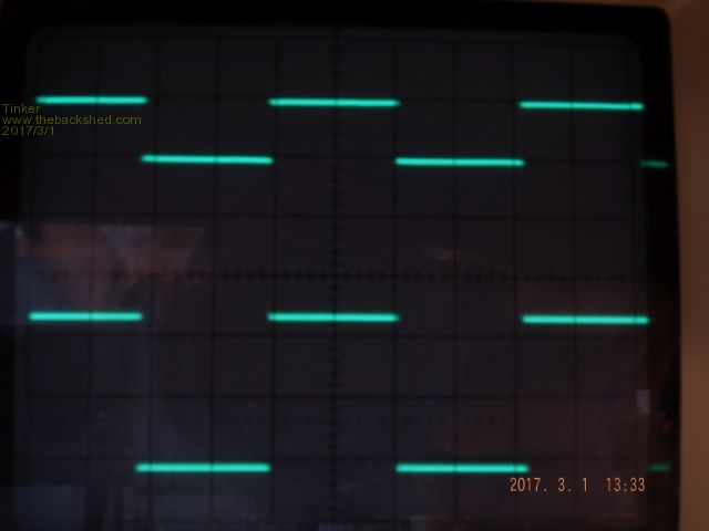 Its too difficult to see the 1us dead time but the traces have no visible overlap. Pics from the high frequency side did not turn out sharp and made little sense to me: 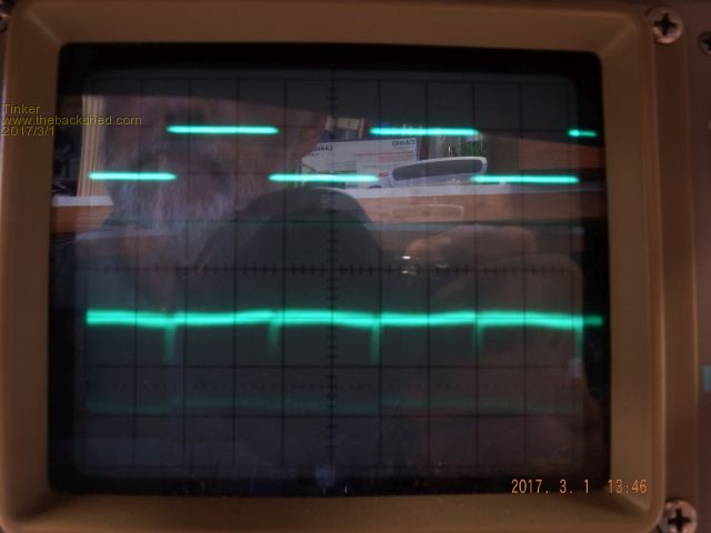 Here's the signal at the capacitor (LO side chip, 1LO) I'd connected to the TC4452 output: 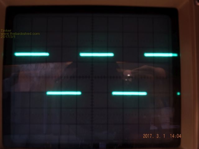 And here the same at the capacitor (LO side chip, 1HO) 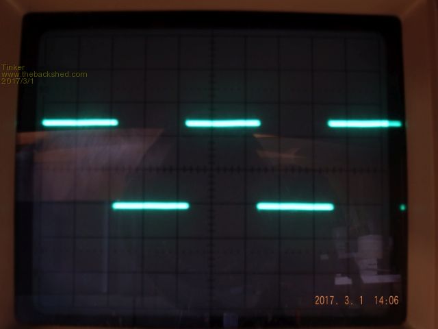 Any comments are welcome, as usual. Klaus |
||||
Madness Guru Joined: 08/10/2011 Location: AustraliaPosts: 2498 |
Today I was testing TC4452 driver PCB's I have made to add to the existing 24 FET boards I have. I did not get to try driving the MOSFETs yet as other things got in the way as usual. I did get very good waveforms at slightly high levels than the input from the IR2110's. Klaus if there was any shoot through, ie no dead time it would have to show on your CRO as spikes. You will need to drive some FETs to try this, as Oztules mentioned using a test board with no caps and a series resistance on the power supply won't blow FETs if the signal is crap. This has saved me a few times now testing the control boards and drivers. There are only 10 types of people in the world: those who understand binary, and those who don't. |
||||
| Tinker Guru Joined: 07/11/2007 Location: AustraliaPosts: 1904 |
Yes, that was a good tip, using no caps for testing. I wish I had known that sooner... There is a awful lot of instant energy stored in 60,000uF. I always had used a series resistor BTW. But that resistor only limited the battery Amps, not what the caps could dump instantly. I'll also try to ramp up the voltage slowly as warpspeed suggested. I have some more block Mosfets on order, IXFB420N10T. These were available at US$16 ea for 10 pieces min. or US$20 for increments of two. Still dear (to me) when the exchange rate & postage is included. I think having just 4 blocks that can handle 200A (terminal rating) is plenty for my inverter. They will run at less than 1/4 of that most of the time. I am quite fond of my alu bar design, too bad I blew the Mosfets by being too keen to turn it on full. A tip, if you want a silent choke then the ferrite toroid is the way to go. But get two of the 120mm OD and stack them. I can get 6 turns of 20mmsq, 4 in hand, tightly wound on. A single ferrite ring gives a slightly higher idle current than my noisy E-core with 4 1/2 turns. Klaus |
||||
Madness Guru Joined: 08/10/2011 Location: AustraliaPosts: 2498 |
The caps give the knockout blow with them onboard the resistor can't help. I have found that when I have had the Inverter working fully and then failed it does not even take out the 300A fuse I have. It just blasts the FETs to pieces and the FET legs vapourize. I don't think the fuse is at fault, just all that power sitting in the caps. There are only 10 types of people in the world: those who understand binary, and those who don't. |
||||
| Warpspeed Guru Joined: 09/08/2007 Location: AustraliaPosts: 4406 |
Great stuff guys. Yes you need a current limited supply without any brutal energy storage capacitors, and any really violent shoot through current spikes should really stand out. There are also some tests you should do on the microprocessor board to make sure the designer did not screw up with that. The problem with any software operated device is that it needs to logically follow one instruction after another without the program crashing. Any idiot can write software that runs, but how it starts up and shuts down under very marginal power supply conditions can lead to the not unknown problem of "blowing up" every now and again for no apparent reason. So connect up the microprocessor board to an adjustable 0 to +5v supply, and run your power bridge through a very small fuse at low voltage. Just enough so that if the gate drive waveforms go momentarily spastic, the fuse will blow without doing any real damage. Then try VERY SLOWLY increasing and decreasing the five volt supply to the microprocessor. If the circuit designer was on the ball, you should be able to do this all day without any mishap. The processor should have an under voltage sensing chip that holds the processor in reset until it has sufficient supply to start running in an orderly way. That is almost never a problem. What can be a problem is if the voltage sags and the software crashes. Getting it to always shut down in a safe manner can be a bit more challenging. If it does go pop when you turn the power off, you will never know until next time you turn it back on. "Oh it blew at power up". Maybe, or maybe it really blew at last power down. No way to really know for sure. So give it the power starvation test, and then at least you can have a bit more confidence in something someone else has designed. Cheers, �Tony. |
||||
| poida Guru Joined: 02/02/2017 Location: AustraliaPosts: 1464 |
Tinker, where can I obtain the 120mm toroid? wronger than a phone book full of wrong phone numbers |
||||
Madness Guru Joined: 08/10/2011 Location: AustraliaPosts: 2498 |
Aliexpress details are in a link on page 25 of this thread. There are only 10 types of people in the world: those who understand binary, and those who don't. |
||||
| Tinker Guru Joined: 07/11/2007 Location: AustraliaPosts: 1904 |
A bit more fun with testing today. First I rigged up My little gate driver boards to some 4110 Mosfet chips and connected the lot into a full bridge inverter. 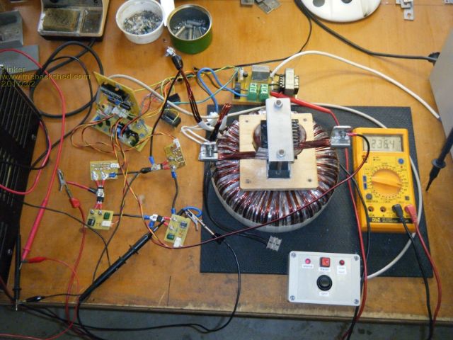 The close up pic below shows the little DC/DC converter blocks I use for the high side power (top right) 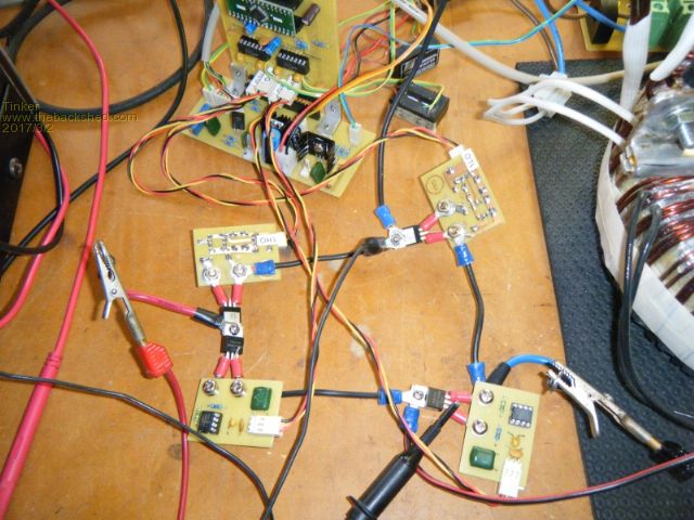 Then all was powered up, voltage & current measured and I got a nice AC output on the scope. 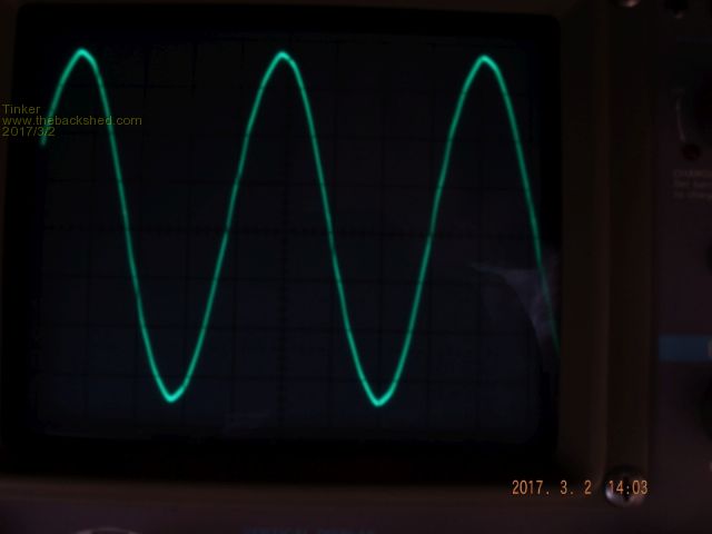 While I was probing around with the CRO probe the inverter just died suddenly. No bang thanks to no caps fitted and limited current supply. Turns out just one of the 4110 chips had developed a D-S short. No idea why. Replacing that one all worked again, of course with no load since there is no heat sink. So far I could not get it to fail again. It occurs to me doing a soak test for each chip might be a good idea, especially if there are 4 or more in parallel in the final inverter. So I'm making a little 4 chip test rig with screw type terminals for quick Mosfet connection. The 5mm spaced terminals will suit the HY4008 chips perfectly. No caps, no heat sink, just for checking the reliable operation and supply voltage endurance. Leaving each set of 4 on for a few hours, with many times on - off switching, should weed out the crappy ones. I think I'll continue using the gate driver chips for the HY4008 experimenting. Even the 4110's took the extra gate drive through a 1 Ohm resistor with no complains. Klaus |
||||
Madness Guru Joined: 08/10/2011 Location: AustraliaPosts: 2498 |
I had a similar experience today testing TC4452's I found 2 FETs in the board were 30 ohms RDS last time I tried that board it worked. They are cheap 4110's, makes you wonder. I have a packet of them that just arrived that are from the same supplier that Oz uses. I will see if the behave any differently. There are only 10 types of people in the world: those who understand binary, and those who don't. |
||||
| poida Guru Joined: 02/02/2017 Location: AustraliaPosts: 1464 |
Thanks for the info re toriod rings, Madness. I want to share some information about the operation of the EG8010 I have discovered today. It seems some people here might want to know how a bit more about how Vfb works. I performed a simple test, feeding Vfb with a DC signal at about 3.05V with a short 1ms pulse 90mV higher. I sweep this short pulse over the entire 50 Hz time frame. I thought this might show how the EG8010 samples Vfb and when it samples it. Or maybe it will show that the EG8010 samples Vfb many times throughout a 50Hz cycle... I knew that Vfb was only looking at DC, from earlier tests as outlined in the EGS002 manual on page 5. I suspected that Vfb was sampled within a short or narrow window each 50Hz cycle. This experiment shows that this is the case. I made a video showing a complete sweep of possible sample times of a 50 Hz cycle and you can see exactly when and where the pulsed input of Vfb effects the output. Right at the top of one half of the 50Hz output. Pulses as narrow as 1% of the 50Hz (i.e. 200ns) clearly effect the PWM output. See https://youtu.be/SdkPxG5mNOY for the results. Our voltage feedback designs will need to take this information on board. I believe Vfb is sampled only within a very narrow window, maybe 200ns each 50Hz. On another forum I posted my findings from playing with a pure sine wave inverter prototype I built using an Arduino to produce the needed PWM signals, as well as have the arduino control output voltage via a closed loop system using a PID control. It works beyond expectations and is stable under all my test conditions. See http://www.anotherpower.com/board/index.php/topic,1228.msg13170.html#msg13170 The point I want to make is that in the arduino code, I sample the output voltage only once per 50Hz cycle, and perform the PID feedback control on that data point only. It seems that this is the way to go.  wronger than a phone book full of wrong phone numbers |
||||
| The Back Shed's forum code is written, and hosted, in Australia. | © JAQ Software 2026 |