
|

|
Forum Index : Electronics : Nano Power Inverter - Roll Your Own Style
| Author | Message | ||||
| Solar Mike Guru Joined: 08/02/2015 Location: New ZealandPosts: 1203 |
Fod3182 is an excellent generic device for H-Bridge drivers 3A, 50-210ns switching, variance any 2 devices = 90ns. With your scope you could easily match them up on a plugin breadboard, prior to running them live; that variation could stuff up dead timing. Si8261BBC-C-IP is PDip plug in replacement, Si8261BBC-C-IS is the SOIC version, both with 8v under voltage lock out. 4A, 20-60ns, variance between devices = 25ns. The Si device has superior spec's for matching multiple drivers. Last I looked RS still have some in stock. Cheers Mike Edited 2021-10-31 21:17 by Solar Mike |
||||
| wiseguy Guru Joined: 21/06/2018 Location: AustraliaPosts: 1267 |
Thanks for the info Mike. If the theory of the differences in the optos being the culprit, causing the grunt is correct, I have been playing with the figures to see worst cases. After a short study of the data sheet & playing devils advocate on all the extremes of the Si8261BBC specs working against you I calculate a potential worst case difference between 2 units of 218nSecs. This is small fry compared to the FOD3182 which comes in at ~530nSecs and they don't publish max and min values for rise and fall times only typical times were used for the calc. By the way the 90nsec diff part to part is actually twice as bad, its +/- 90nS. The Si8261BBC is a nice part but its simulated reverse diode voltage is -0.3Vmax. I am using Warps inverse optocoupler drive so the board would need a bit of redesign to work to its best performance. I reckon my best option without a redesign is to match/select the optos. The small capacitance that is used for the dead-time which is in parallel with the optos might also need to be selected/matched, they can be +/- 20% depending on the type & specs. I have reversed the high side optos on my inverter and will finish reassembling it today, will be interesting to see the result. hopefully I am now on the right track to solving this grunt, time will tell... If at first you dont succeed, I suggest you avoid sky diving.... Cheers Mike |
||||
| Warpspeed Guru Joined: 09/08/2007 Location: AustraliaPosts: 4406 |
I remain unconvinced. This is all well trodden home brew inverter ground. The thundering heard have been building grunt free inverters of very similar design using similar parts for a very long time. Something rather unique is at work here, its a problem nobody else seems to have had. It will end up being something very simple and totally unexpected. Cheers, ĀTony. |
||||
| wiseguy Guru Joined: 21/06/2018 Location: AustraliaPosts: 1267 |
I'm sure not many of these well trodden thundering herds are using an inverse coupled optocoupler drive using the FOD3182 driven by the nano code (apart from maybe Murph) and with my deadtime, layout and my (ultra?) low impedance 3xsendust stacked choke/2xtoroid setup and 13+ AMP FET drivers with 2R2 gate resistors? Obviously something in the above lot must be causing this issue. Also when you suggested that 2 x RC filters should give 2 x sinewaves, not in the configuration we are using, this would result in 2 x half sinewaves 180 degrees apart. LHS is held at GND whilst we PWM RHS. Next hold RHS at GND & PWM LHS. When reassembling my inverter I accidentally reversed an 8 pin connector and promptly took out 2 resistors and killed 2 optos, one that I had just swapped! - which negated a bit what I was hoping to see, I actually got out of it quite lightly. Any way Tony as you predicted after replacing the optos & swapping the optos around did not seem to influence anything by any measurable amount, note I did not try swapping the dead-time capacitors across the optos, but I cant see them influencing much. All CRO scans below are 1 sec/div You can see the grunt starting well before the end of ramp it typically seems to kick in at about 70-75% of soft start ramp Typical startup energy envelope with grunt. 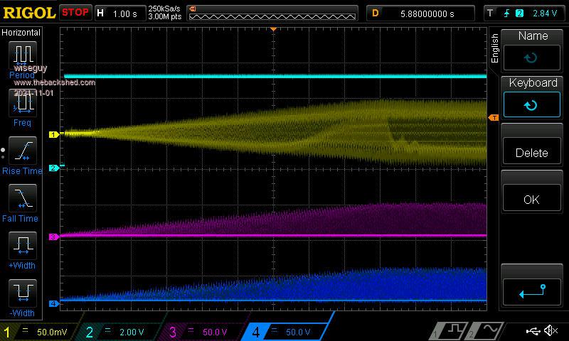 Reverse transformer after above capture soft stopped. 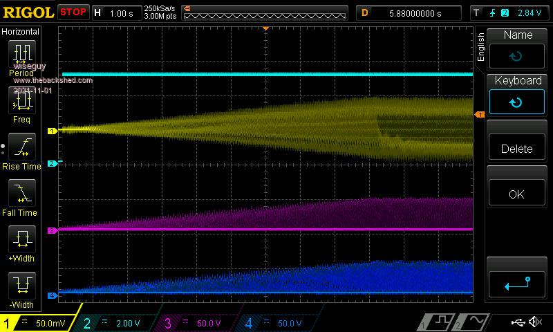 Second soft start after transformer reverse - back to normal shape.  Run same test with 80 milliOhms of series R  Run same test with 200 milliOhms of series R 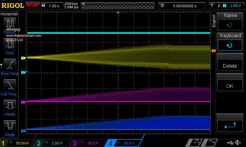 With more than 100 milliohms of series resistance in the choke transformer primary circuit the envelope looks pretty normal and there is no sign of grunt. This outcome is obviously quite unacceptable. I have exhausted my current ideas & have no idea what to try next, so for now I will shelve it for a few days, time for some alcohol maybe lots of it ! Edited 2021-11-01 17:40 by wiseguy If at first you dont succeed, I suggest you avoid sky diving.... Cheers Mike |
||||
| Warpspeed Guru Joined: 09/08/2007 Location: AustraliaPosts: 4406 |
Best just to walk away from it for a while and relax a bit. Some fresh thoughts and ideas may come to you. Cheers, ĀTony. |
||||
| Murphy's friend Guru Joined: 04/10/2019 Location: AustraliaPosts: 674 |
Mike, could it be that you made your inverter a wee bit too complex?   Below are two schematics of my 6KW opto isolated inverter which I built to your original schematic but with quite a few parts omitted. It is completely silent on start up or shut down (I never start it with any load). 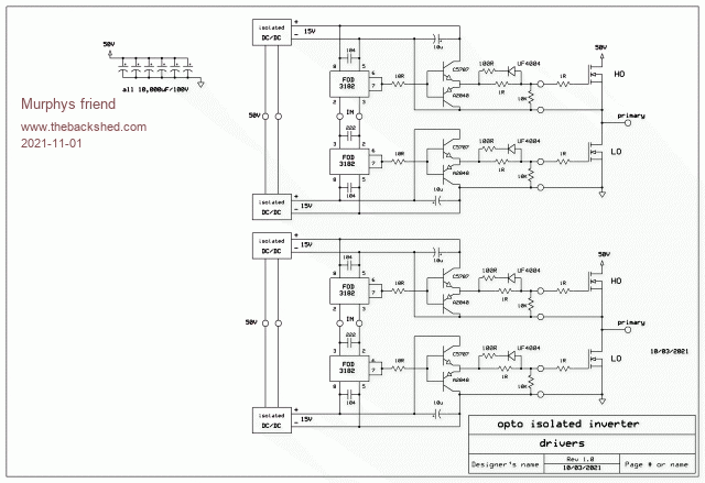 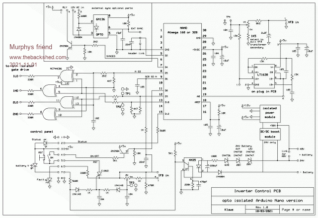 I do not have a CRO capable of seeing tracces like the ones you posted BTW. |
||||
| wiseguy Guru Joined: 21/06/2018 Location: AustraliaPosts: 1267 |
Hi Murph, The main difference between my build and your (and others) build as I see it is the choke. Your power stage certainly looks very simple when you omit the other dozen or so FETs  Ok I admit to some "complexity" but they are not related to the issue of the grunt, they give me some extra features that I wanted (no grunt does not count as a feature) You also have an active filter in yours but as I've tried two totally different feedbacks with identical results I'm sure its not that. Did I take too many turns off my main toroids, from memory I wanted 235V out from low battery of around 44V, and that was the winding ratio I used ~ 1:7.5. The gain is wound back a fair bit running from 48V I guess open loop it would be around 255V maybe my feedback is still too slow and it over drives briefly. I love Sendust chokes and how efficient and cool they run with 50 - 100kHz+ frequencies it just laughs at you. That is when its not grunting apparently....... If I had used Iron and wound lots of turns I suspect I would not have a grunt. But my challenge now is how to make them work for me. I'm not beaten yet but I do need some space from it for a couple of days so I can regroup and tackle it again. Starting an inverter unloaded giving it a short spell before connecting the load is very wise. I am thinking of more complexity and adding a zero cross type relay so it connects the load at the zero crossing. (it then shouts "suprise"). Then a relay of course to bypass the zero crossing losses - dont you just love complexity haha. Edited 2021-11-01 21:10 by wiseguy If at first you dont succeed, I suggest you avoid sky diving.... Cheers Mike |
||||
| Murphy's friend Guru Joined: 04/10/2019 Location: AustraliaPosts: 674 |
You are right, drawing in those extra mosfets does mess up a simple schematic  so I left them out. so I left them out.FYI, the 6KW inverter has 4 parallel mosfet strings (16 units) and the 3KW one only 3 (12 units) in parallel. I use removable little PCB mosfet carriers nowadays, have blown up way too many to solder them directly to the big PCB any more. The little circles in the schematic shows where they connect. Funnily, ever since I used yours and warpspeeds inverter ideas the blowups have vanished, its definitely a winning design as far as I'm concerned. I use a re cycled Aerosharp choke core. |
||||
| wiseguy Guru Joined: 21/06/2018 Location: AustraliaPosts: 1267 |
Murph, for the value of others thinking of copying your circuit, I may have said this to you before, but the correct value of the 4 resistors from the gates to the LEDs should be no higher than 150R for VCC 5V. The data sheet specifies a recommended current of 10mA despite their typical 3 - Maximum 7.8mA threshold on current at a forward voltage of maximum 1.8V. The value is determined by ((5-1.8)/.01)/2 = 160R so 150R is the nearest preferred resistor values and resulting LED current is 10.6mA. However there is a further consideration, the recommended SN74LV86A data sheet suggests that guaranteed output voltage at VCC 5V and supplying 12mA will be ~4.3V. Taking that into account now the sum becomes ((4.3-1.8)/.01)/2 = 125R so 120R is the calculated worst case recommended resistor for the 4. If you get a best case FOD3182 opto/s with 1.1V min forward voltage the LED current for 120R would be ~ 13.3mA. Well within their recommended operating range of 10 - 16mA. In my much simpler nano Pico board, which is a work in progress - its essentially finished except I am holding off releasing it until I am happy it doesn't contribute to the grunt, there are little TO92 PNP & NPN buffer transistors at each gate output, which can be fitted so more feeble gates like the 74HC86 series can easily drive the opto LEDs. If the SN74LV86A is used though they would not need to be fitted. If at first you dont succeed, I suggest you avoid sky diving.... Cheers Mike |
||||
| phil99 Guru Joined: 11/02/2018 Location: AustraliaPosts: 3158 |
Some more things to take on your Contemplation Retreat. Zero crossing switching is good for resistive loads, ideal for capacitive loads but worst case for inductive loads. For them lowest inrush current occurs when switched on at the peak of the voltage in either half cycle. So it depends on what the biggest load is likely to be at startup. A reasonable compromise is around the 135 degree mark (2 to 3mS after Vmax). The "trim" experiments showed that the grunt can be altered. So perhaps dynamic adjustment of the trim in response to feedback of the primary current might actively suppress the grunt. By comparing the peak current of the current half cycle with the peak of the preceding half cycle and applying a trim of 1 unit (in the appropriate direction) if the difference is more than say 10% or by 2 for 15% etc. it could prevent the current peaks growing excessively, without affecting normal operation. |
||||
| wiseguy Guru Joined: 21/06/2018 Location: AustraliaPosts: 1267 |
Thanks for your comments Phil & I agree totally with your thoughts. In my house, apart from the dreaded compressor, all fridges and other loads are power factor corrected type loads and in all honesty a compressor is the least likely item to be used whilst on inverter power & even so it has proved in the past that as long as the inverter is started and running THEN turn the compressor on it has always worked perfectly. It initially took a lot of hard thinking to get my head around maximum current at zero crossing but it eventually gelled despite being a bit abstract. Whilst doing the mental Gymnastics if the inverter primary is supplying current which at the peak of the current sine is actually the zero crossing of the 240V at the secondary what does that mean then if we put an inductive load on the output of the inverter, does that mean that the peak current of the load now corresponds with minimum FET current - AC thinking hurts my head. I also agree with your comments about predicting and compensating based on primary current, but I would need to be a software programmer extraordinaire to achieve that. I am wondering what I may be able to do in an analog/discrete fashion, that is how I have got by over many years of being software challenged. Maybe I could make a discrete trigger delay based on a number between 1 & 256, that way I could set the pulse number I wanted to see in the train for each 180 degrees and compare it to the corresponding pulse of the next 180 degrees to see how well they are matched. If at first you dont succeed, I suggest you avoid sky diving.... Cheers Mike |
||||
| Murphy's friend Guru Joined: 04/10/2019 Location: AustraliaPosts: 674 |
You are quite right, I have corrected the values on my board but neglected to do so on the schematic. Call it a senior moment.. Or was it done to giver those copy cats a tough time?    |
||||
| wiseguy Guru Joined: 21/06/2018 Location: AustraliaPosts: 1267 |
Ok I have wiped the cobwebs from this post and decided to add some more. I apologise in advance for what will be a verbose post, I have written most of it but will only drip feed it out over a few posts. The forum has been very quiet lately and it leaves me wondering if anyone actually builds boring old single phase inverters anymore ?? It is good to see the interest & experiments of some though, delving into three-phase units. I still have unfinished business with my inverter, after not finding a simple solution to the "grunt" on startup I decided to take a break for a while and rethink my approach. I had killed my inverter briefly, after trying to start the inverter into a compressor load during soft start - not the wisest decision of the week, it grunted and went bang. Despite the fact that even with a grunt at startup, as long as the inverter was given a few seconds to stabilise after starting before attaching the load it always ran perfectly. One dead shorted high side FET and four low side FETs fixed it. I have never really liked what I don't understand and I didn't consider the grunt a desirable feature so it had to go. If it was not explainable then it was also not understood and the various tweaks etc for different fundamental SPWM frequencies and ramp times etc all affected the grunt but did not eliminate it or draw us/me in a particular direction. The only "cure" I found was to insert a resistor of at least 0.5 Ohms in series with the toroidal transformer, the grunt was finally eliminated at ramp up completely. Now after ramp up the resistor could be shorted out and life would be good again - or would it? For a few years now I dreaded the scenario of my not being home and the inverter tripping out and needing a restart. Now giving phone instructions, look dear wife just press button A for 5 seconds then turn switch B on then wait 3 more seconds and operate switch C now turn on circuit breaker switch D and all will be fine, then later waking up in hospital half beaten to death with a frying pan..... That is why way back in the early days I proposed a simple on off switch to the inverter. Let the controller make the decisions of when to close the main contactor ramp up, attach the load etc. it was met with less than enthusiasm here but it was the approach I have adopted. The second part of designing a roll your own inverter is that if it worked well and anyone else wanted to build up their own unit, testing it and repairing it without special tools or knowledge was a must. So Roll your own Inverter project MK2 revised. I decided to attack the issue on two fronts, one that I had control over and 1 that relied on someone elses software. 1) Explore use of EG8010 in inverse optocoupler drive power stage. 2) Explore the use of an STM32 Nucleo module for PWM generation with appropriate code creation. More tomorrow..... If at first you dont succeed, I suggest you avoid sky diving.... Cheers Mike |
||||
Revlac Guru Joined: 31/12/2016 Location: AustraliaPosts: 1239 |
Mike, Just a thought, some of us were happy enough just get a home built inverter up and running to start with, (as I have been) I do agree though, a single on/off switch for the inverter is a good option especially if at times it needs to be operated by someone other than the one that built it.  I have seen a few commercial inverters with the single on/off switch, but have not worked out how some of them work, some have less capacitors and leave it to the user to find out what splatting the terminals or switch really is....surprise is the first reaction.  I think a separate (cheap) micro controller can take care of the capacitor charge, start up and close a relay when AC output voltage has been reached, Actually it might be better if it had set time, well after soft start has been completed just to be sure. Not sure the best way to do the capacitor charge and close a contractor after, could this be done with solid state to some fashion? If all this could be done using a micro and easy to get parts, it might be something that could be retrofitted to any of these inverters. Just an idea and would not be the first.....good chance your already working on something better.  Interesting. Will be watching with interest. Cheers Aaron Off The Grid |
||||
| wiseguy Guru Joined: 21/06/2018 Location: AustraliaPosts: 1267 |
I asked a clever software engineer at work to take a look at Poidas Nano code to see if anything else could be squeezed out of it. The Nano with Poidas software had some rogue minor pulses at the beginning of each 180 degrees that appeared in the wrong direction just before the zero crossing. Poida told me that essentially he had exhausted the capabilities of the Nano and it could not be fixed easily iff at all, and it was of a minor consequence and plenty of builds unit were working just fine. The software engineer agreed to help but the proviso was he would only use an STM32 approach, being his processor of choice. He believed that it would be faster and more effective with better results than learning understanding and modifying existing nano code, the nano not being his forte amongst other reasons. We chose a NUCLEO-L432KC which was very Nano-ish in that some nano shields could be run as it had a lot of nano functionality. ĀHowever there are multiple differences, the outputs are 3V3 not 5V and some pins are preassigned for tasks ie onboard LED and port pins not able to be used as they couple to other pins to emulate IIC functionality. In short even though possessing similar nano pin outs it is a different beast and not simply interchangeable. I have always envisaged a simple small switch to turn the inverter on and off, with all capacitor precharge and high current switching automated in the process. ĀI purchased a Kilovac 900V 500A solenoid with 24V drive to achieve this, the 24V unit was much cheaper than a 48V unit ~ $115AUD at the time. Most high power inverters will be required for 48V, some will use 24V and some will want to use a higher voltage than 48V, even 12V can be supported, nothing in this inverter design precludes all 4 variants with only some minor component value variations required. I will ignore the choke and transformer requirements for the different inverter supply voltages at this stage as obviously there are different specs for these major parts required. My Mark1 inverter required the use of a sub PCB for the gate drive power supplies, the new Mark2 design incorporates little readily available power modules as part of the main PCB. There are quite a few options available for the Power PCB with regard to gate drive power and provision was made for the small 1W NME12/12 or larger 2-3W 12/12 or the AC/DC vertical modules or a mixture of them. ĀProvision has also been made for a negative gate bias for the lower side FETs when not being driven. ĀThe negative bias happens automatically if you use a 15V low side power supply module. ĀThere are two isolated power modules required for the LHS & RHS high side bridge gate drives. One common power module is shared by LHS & RHS gate low side drives. In my experience 12V gate drive is perfectly adequate for Power FETs. Most are specified at 10 volts for lowest on resistance, nearly all FETs I have played with exhibit lowest RDSon from 8+ volts. If using negative bias the low side power module DC output must be a 15V (or 18V) output for the approx -3V (or -6V) negative bias. Now for a more detailed explanation of the circuits operation. When the small switch is off the inverter circuitry is galvanically isolated from the main battery supply power. When the small switch is turned on simultaneously power is applied to the micro controller, gate power modules, and via a precharge resistor the main power module FETs with its Bulk capacitor/s is monitored. The microcontroller now waits until the ĀBulk capacitors are ~98%+ charged and then the Kilovac is driven and applies full power to the Power bridge. The microcontroller drives the Kilovac with different PWMs for initial pull in and then hold in currents for increased efficiency. After the Kilovec is driven the controller then applies a ramping sine pwm (SPWM) to the Power stage. ĀNote the Kilovac is a 24V unit running from 48V but PWMed for 24V pull in and 8V hold in. When powering down the inverter, the small switch is set to "off", which signals the micro to ramp the SPWM back down to zero. Then the main contactor is opened (under no current) and the inverter "dies" and is galvanically isolated again. ĀOnce the shutdown is initiated even if the small switch is turned on again a full shutdown of the output AC will occur before the SPWM ramp up begins again. A suitably rated DC overcurrent breaker is recommended as a matter of course between the main battery supply input and the Kilovac solenoid. I would advise that it is prudent to wait for the inveter to have ramped to the controlled AC output before turning on the AC output circuit breaker to whatever load is going to be driven, especially for compressors and the like. ĀI have not made provision for auto switching (enabling) the AC after the output is stable and the ramping has finished but it would be a simple add on. The Power pcb of the inverter MK2 was also designed to ensure it could utilise the enclosure and heatsink of the BP/SunnyBoy/Aerosharp etc style of grid feed inverter. ĀThe Power PCB has a relatively low profile so most of the internal space is still available within the enclosure for the choke and transformer and small 100mm x 100mm control board. Whilst waiting for the Nucleo code to be written I decided to create a controller using the controversial & notorious EG8010. Whilst I initially despised it with a passion I cant deny that some swear by it and there are many inverters using it with various degrees of success world wide. Using the inverse optocoupler technique that Warpspeed liked I initially used a Nano so I didnt have to deal with the cross conduction and othe glitches of the EG8010. ĀAlso the EG8010 did not output my preferred transformer drive that the nano uses. I had a good experience with my first inverter despite its foibles it easily ran my whole house in the absence of mains power and became luke warm in doing so for some hours of kettles, toasters, microwave, Oven, fridges lights etc. some concurrently. The inverse opto drive method for power inverters has proved reliable and robust to me. So I decided to configure a few parts around the EG8010 to get a nano type output and added my precharge and solenoid drive to it and made the connector pin outs for the Nucleo and EG8010 controllers interchangeable. Using this approach I had something to play with whilst waiting for the Nucleo code. Edited 2022-06-16 19:15 by wiseguy If at first you dont succeed, I suggest you avoid sky diving.... Cheers Mike |
||||
| wiseguy Guru Joined: 21/06/2018 Location: AustraliaPosts: 1267 |
Thanks for the comments & input Aaron some points I believe have/will be addressed. whoops some duplication now deleted I have also been curious to see how the EG8010 would perform using an inverse optocoupler power stage. The native EG8010 has some glitches that have the potential to cause a shoot through event but using the inverse opto drive makes this event impossible. So along with the STM32 Nucleo controller PCB I also created an EG8010 controller PCB which uses the same plug pinout for plug and play ability for A/B comparisons. In some previous designs on the back shed I dont believe the EG8010 voltage feedback was implemented for best performance. The data sheet suggests that after a load change the output should settle within 3 cycles. ĀAll their schematics apply the output waveform to a resistive divider which is not rectified/filtered and feeds it back to the controller. It looks at the peak of the sine waveform and adjusts the control circuit to compensate accordingly to maintain a constant output. A small 2mA/2mA voltage transformer is used to feed back the mains voltage sample to the controller. The feedback signal is fed to a precision rectifier and an amplifier with a gain adjustment pot, to set the output ACV. Note this is not a DC level but resembles a full wave rectified series of 180degree positive half sinewaves all joined at 0V. The EG8010 controller SPWM outputs are gated with 2 x PNP transistors to achieve the same 180 degree output drives that the Nano creates. The controller card also has a heap of settable 0.1" links for testing and implementing various deadtimes, 50/60Hz, Unipolar/Bipolar drive, inverted drive, variable frequency drive etc. I use zero dead time for the EG8010 as the inverse opto drive uses a capacitor across the LEDs of the gate driver optos to control the dead time for each half bridge. The capacitor I used is 1nF, and series resistance totals 120R, from memory it gives a few hundred nanoseconds of dead time. Its time to post a picture of the 8010 working as an inverter. The mains output and feedback to the EG8010 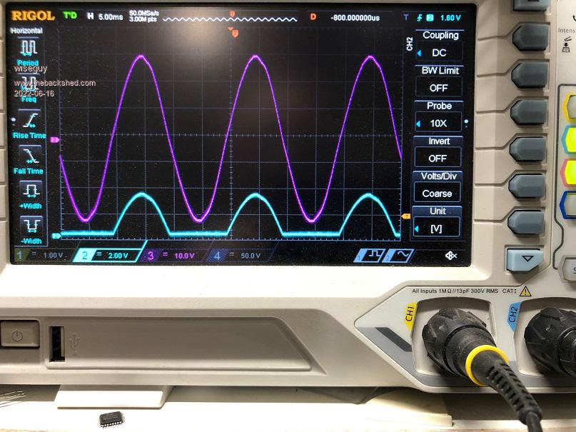 The test bed 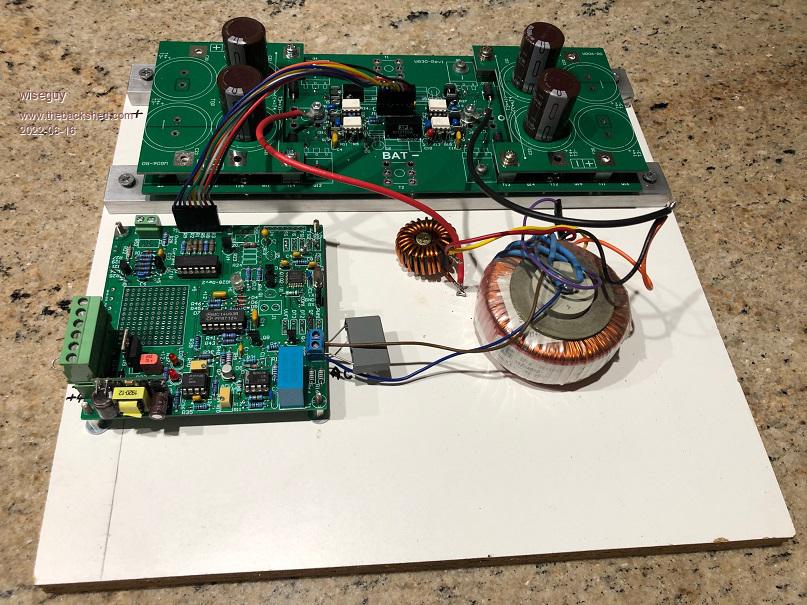 The distortion at the peak of the sinewave is due to the 2 Power-Mate loads I had attached which use a charge pump circuit and it is a very small toroidal in my test bed. A figure of interest the transformer is a 12V toroidal. With a 21V DC supply to the Power FET stage and output voltage of 235V it drew a whole ~45mA of current from the 21V supply !! I was curious about the feedback so I reversed the toroidal primary and the result is - it went apesh*t! So I Āwas just lucky to get the phase right in my first connect. I intend to use a precision rectifier so the feedback in the first picture above will not have a gap between humps, then it will not matter about the phasing - I believe this was the reason they full wave rectified their transformer feedback implementation. Edited 2022-06-16 20:23 by wiseguy If at first you dont succeed, I suggest you avoid sky diving.... Cheers Mike |
||||
| wiseguy Guru Joined: 21/06/2018 Location: AustraliaPosts: 1267 |
Unfortunately (fortunately?) I don't have the terminals and FETs to fully populate the Power PCB yet. I decided to use the HY5608W FETs for the power stage and I only had 10 on Hand, I need 16, the rest will be here soon. The HY5608 FETs are rated at 80V and 360A at 25 deg or 250A at 100deg & pulsed current 1290** amps. Not sure about the ** I think it is their way of saying ok go ahead prove me wrong.... We also need to remember that it is probably metric amps not imperial amps. The gate rise times (1 FET loaded per leg) with gate resistor 2R2 was measured at around 100nSecs rise time. ĀSo I cant drive the inverter power board to full power for a couple of weeks but I must say the EG8010 & power PCB performs far better than I expected. Will it run ok at 5kW ? time will tell. The control board has 2 comparators, to check the input voltage and the bulk capacitor voltage. This drives 2 LEDs so if the Kilovac solenoid is not your thing it can still have a pre-charge push button with LED indication that they are charged. Full manual operation is possible, it just has extra bells and whistles if you want to load the extra parts to the controller card and have it automated. Ok I'm done writing for a little while. In the next instalment I will post and describe the circuit and how the Power stage is mechanically built with pictures and descriptions. I have minimised tapped holes for FET mounting with a novel buried nut concept that works a treat and saves a lot of time and simplifies repair if it is ever needed. Edited 2022-06-16 23:42 by wiseguy If at first you dont succeed, I suggest you avoid sky diving.... Cheers Mike |
||||
| wiseguy Guru Joined: 21/06/2018 Location: AustraliaPosts: 1267 |
Latest Power Schematic PWR schematic.pdf Nucleo Controller Schematic Nucleo Controller.pdf EG8010 Controller for Inverse Opto drive New 8010 Inverse LED Controller.pdf Front Nucleo controller PCB Rear 8010 controller. Note the 8 transistors and other resistors and connector not loaded on the Nucleo is for when you want to use a cheap 74HC86 in lieu of the 74ACT86 exclusive or gate and still drive 2 x Power PCBs. 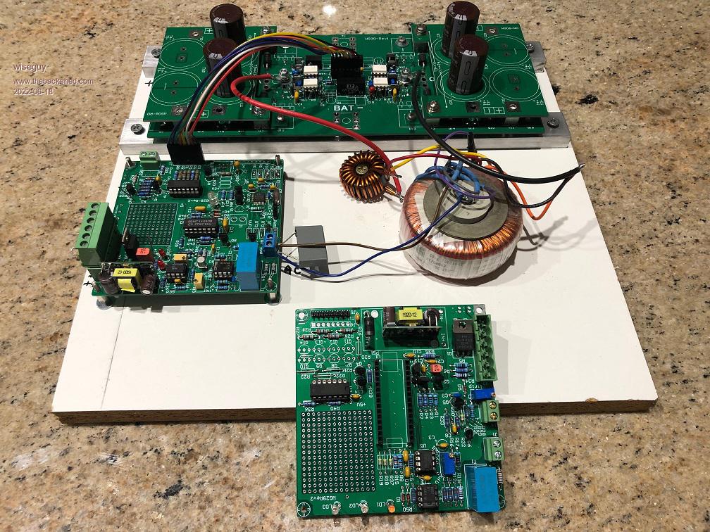 Aluminium Bar drilled ready for Nut inserts - yes the FET holes are 1.5mm offset from the centre line to ensure the heat conducting FET face was not right at the edge. The 2 x M4 holes close to the centre of the bar was for extra mounting/pull in to the heatsink, probably both not needed or just one central one would suffice. 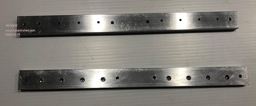 Power PCB screwed to Alum. bars for heatsink M4 Tap centres 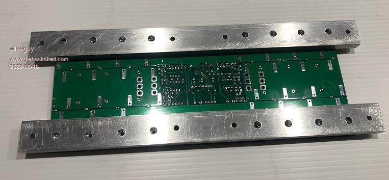 Holes tapped for heatsink mounting. Note separate cap PCB, has 4 x 1000u caps fitted for trials, final will have 4 x 8,200uF 63V caps fitted 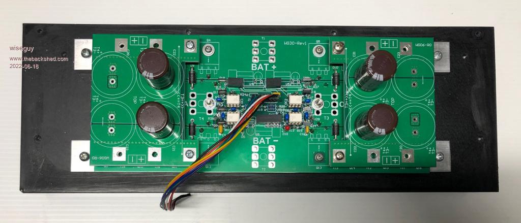 PCB Current carrying Traces Raw PCB image 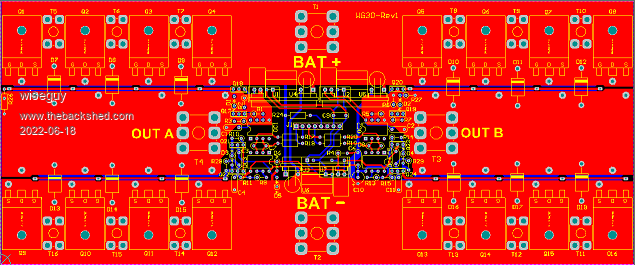 FET mounting with Drain ferrite bead and Gate resistor. 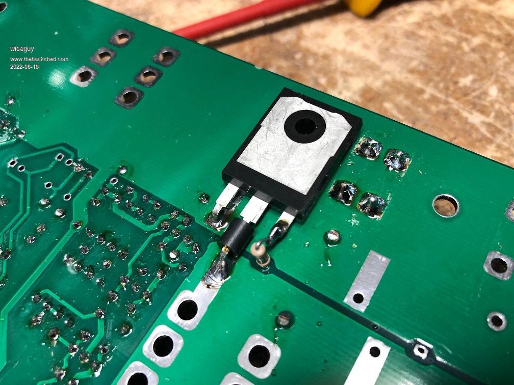 Image of Gate Power modules for 48V in 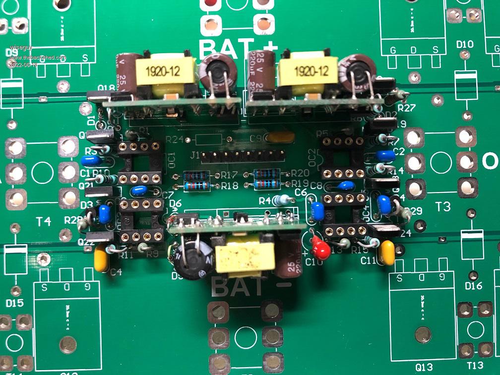 Image of High Side Gate Power modules powered from 12 on controller. Note lower Gate drives can also be a 12/12 0r 12/15 module - required for 12 & 24V versions. 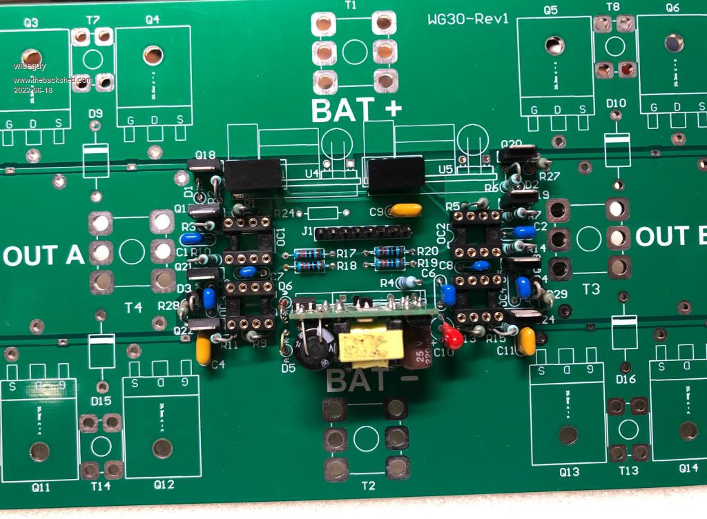 HY5608W datasheet - do I really need 4 devices per leg for 5 KW? maybe only 2 or 3 required? HY5608W.pdf The main power PCB is 260mm x 108mm. Power traces are all ~ 34mm width top and bottom of PCB (68mm total). For a 10 degree rise above ambient a 34mm trace is rated at 51.5A, for 15 degrees above ambient 61.6A. The combined traces are either 103A or 123A which at 48V is either 5kW or 6kW continuous, depending on the Temp rise you are comfortable with. For best current into the PCB traces I chose not to use 3 x FET connections in line, instead I staggered the FET terminals to allow the Source and Drain terminals to meet into the full PCB trace width. I also cut the long gate terminal off at the Mosfet just before it widens at the FET terminals shoulder. The gate resistor (I use 2.2R ) is formed to solder into the small PCB hole and to solder directly to what remains of the Gate shoulder/tab. ĀThis allowed the maximising of the current carrying PCB traces. I think it is a bit comical that the TO247 FET gate terminal is sized the same as the Source & Drain, and they are rated to carry pulsed currents of ~ 1290Amps when the maximum current the Gate lead will see for a few tens of nanoseconds is probably a couple of amps, usually in series with a gate resistor of 2 ¢ 10 Ohms. ĀProviding a suitable sized hole and PAD for the normal gate pin on the PCB would reduce the width of the main current carrying copper areas. I mount the Power Mosfets on a 300mm length of aluminium cross section bar 25mm wide, I use 10mm thickness, there is also a 12mm thick extrusion available. ĀThe fine scratches that look like I kicked it around the workshop are essentially invisible to the naked eye but look like gouges when looking at the digital photo.... Prior to using the method outlined below, I used to have to drill and then tap the 16 M3 FET mount holes, which was slow and tedious and always at risk of snapping the tap in hole 8 and having to start afresh. My new method involves drilling an M3 clearance hole right through the bar and then turn the bar over and using the M3 hole to centre the drill, drill a 6mm dia hole that is ~ 5mm deep on the outside edge (~5.5mm at the centre). The M3 nuts I had to hand were ~ 6.1 - 6.15mm at the widest tips of the nut. Now either using a hex head high tensile 3mm screw and alan driver pull the nut into the 6mm hole using the Alan key driver until the nut is seated as far in as it will go. Alternatively use the drill press to push the nut into the 6mm hole - I recommend putting the nut on a screw wound all the way to the head first and then use the 3mm clearance hole and the 3mm thread of the screw to help keep the nut square to the hole as you press it in, then unscrew the screw when finished - it works a treat. Obviously the intention is to use heatsink compound between the mating faces of the heatsink and aluminium bars when finished. Murphys method of using a TAP guide for achieving a perpendicular Tapped hole was maybe obvious but I had never bothered in the past. I decided to create one to try it out using nylon block ~ 30mm thick with a 4.1mm hole drilled through it I donÆt have the luxury of a lathe. When creating 4mm tapped holes now it really speeds up the process as there is complete confidence of the alignment of the TAP to the hole and there is no fiddling and tweaking required during the beginning of using the 4mm Tap ¢ highly recommended. Edited 2022-06-18 11:39 by wiseguy If at first you dont succeed, I suggest you avoid sky diving.... Cheers Mike |
||||
| Murphy's friend Guru Joined: 04/10/2019 Location: AustraliaPosts: 674 |
Thank you Mike, for the endorsement of the tapping guide. I happen to like tapping  , there are often ~100 tapped holes in my inverters. , there are often ~100 tapped holes in my inverters.I have used your clever method of sunken nuts to avoid tapping but mainly in plastic. With a finned heat sink its often unavoidable to tap the hole(s). I'm following your inverter improvements above with interest, presently building a smallish single toroidial inverter with opto isolated Nano drive. In one of your posts above you seem to go to great lengths, using high current DC contactors and whatnots, to switch off & on the inverter. Why? This would only be required for the first start up and possible subsequent re location of the inverter. Once its running, to turn it off I simply switch off the Nano and leave all the big power cables to the battery connected. This keeps the big capacitors charged and, with the inverter not running, the power draw is minimal. Turning the Nano on starts & ramps up the AC and she is ready again to power something. Surely SWMBO would manage a single switch?   |
||||
| wiseguy Guru Joined: 21/06/2018 Location: AustraliaPosts: 1267 |
Hi Klaus, thanks for your comments and question - I do not want to take the enjoyment of tapping a 100 odd holes away from anyone - I am not a total killjoy. ĀUsing the rails and captive nuts means that no tapping is required for the initial assembly. If heatsink tapped holes are needed there is only a few 4? 6? required to mate the rails to the heatsink. The finned heatsink has currently 4 tapped holes to hold the Power assembly FET rails to it. That was 4 too many for me but you are right the fins were not spaced far enough apart for captive nuts - I haven't given up on it though, I think I could find some Hex head screws and grind a bit from opposite sides of the head if/as necessary for the head to fit between the fins then I could have a clearance hole in the heatsink and rail and put a nut on the screw protruding from the rail - voila no tapped holes Ā  Ā Ā There are times I will remove power from the inverter totally using the DC breaker. We plan to travel and be away from home for longish periods of time. I happen to really like galvanic isolation & the concept of being totally isolated from all that energy in the batteries by real air gaps is comforting to me. I forgot to mention that off really means off no surprises internally with charged caps or infinite amps (briefly) to scare the bejesus out of you or worse - assuming that you neglected to turn off the DC Breaker/isolator. As Aaron said, as long as the guy who designed and built it is powering it up from cold there wont be a problem. As I get older (not a long way off....) I worry that I (or someone else) may leave a switch in the wrong position. Besides I hate big splats they scare me. With the contactor & circuitry it doesn't matter whether the inverter run switch is on or off it starts nicely with no splat when the breaker is turned on. Ā When the run switch is off nothing can run, if the run switch is on it just starts the pre-charge to the caps, the contactor only closes automatically when the big caps are fully charged. I should add that my design does cater for a push button pre-charge & if you even want LED indication when they are charged its just a few cheap extra parts to do it. ĀThe powered contactor & components are totally optional & not required. Did you notice the old transistor radio style of vertical resistor/diode mounting. It really helps when you are trying to squeeze lots into a tight space and dont want to use SMD or increase the physical size lol Edited 2022-06-18 16:13 by wiseguy If at first you dont succeed, I suggest you avoid sky diving.... Cheers Mike |
||||
| The Back Shed's forum code is written, and hosted, in Australia. | © JAQ Software 2026 |