|

|
Forum Index : Electronics : building an Inverter from scratch
| Author | Message | ||||
Madness Guru Joined: 08/10/2011 Location: AustraliaPosts: 2498 |
I am no expert, however the parts I have highlighted in blue appear to be in contradiction when you look how the different circuit boards are designed. The tracks from the H-bridge on the opposite side of the PCB have more 20 volts difference to the gate signal tracks. Is there a possibility that there could be a capacitance there, one of those tracks also has 20KHZ on it. If these tracks have no effect it would make sense to make them as short as possible, but the Chinese boards have them as long as they can practically be. There are only 10 types of people in the world: those who understand binary, and those who don't. |
||||
oztules Guru Joined: 26/07/2007 Location: AustraliaPosts: 1686 |
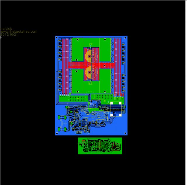
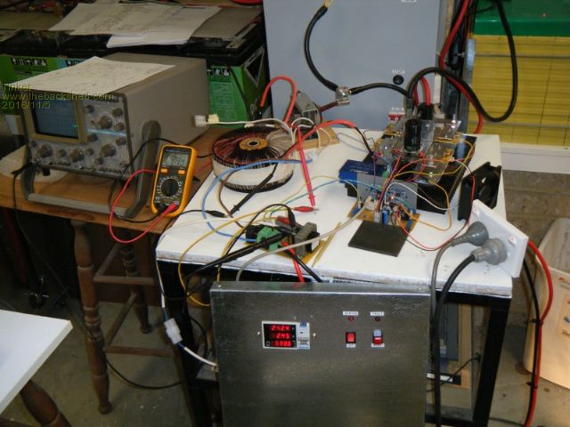
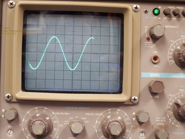
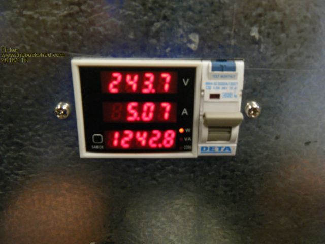
Tinker.... Here are a few pics from this morning.... after reading your woes, I can't put my finger on why.... but here is a few pics showing what I have gotten away with ... with messy circuits spread over a wide area.... but something is right, as it works fine. Here we are with a wide shot showing the carefully laid out inverter under test. It is using that board I showed earlier, with the controller I showed earlier ... somewhere here. Both PCB files are there to send straight to the chinese nanufacturers if you want. This proves that tidy does not mean dosen't work and again..... see sine wave... over 4kw and power meter... The dyne transformer is simply to isolate and bring the 240 down to 32 for the scope... it has an extra 2uf across it because it is used to bench test the boards after I build them.... it help a little bit extra for shaping as I only have 2uf on the board ( little tranny took up the extra space so only one there now). There is a small blip at cross over if you look closely at expanded view, a close up gives only part of the wave because of the crappy camera... and operator who know no better how to use it. ( no zero line is not set ) I figure that if that is the worst that happens at 4kw.... I'm happy Sharp eyes may notice a few little torroid rings there, and this is using a torroid ring from a sharp GTI for the filter... ran out of e cores... seems to work just as well, but other torroid rings in my possession do not work very well at all with low turns on them. Here is another pic of the inverter boards As an aside, here is the solar controller in the background doing over 100 amps That footscray transformer is 2 in hand 25mmsq wire for the primary and 4 in hand 1.8mm for the secondary... so fairly stiff too. ...........oztules Village idiot...or... just another hack out of his depth |
||||
Grogster Admin Group Joined: 31/12/2012 Location: New ZealandPosts: 9936 |
@ Madness - You may well be right. I also am no expert when it comes to high-power MOSFET circuits. I am going on some theory, and what others have told me with respect to high-impedance lines and MOSFET gates. This may WELL change for high-power MOSFET drive concepts over low-power stuff(less then 5A), so what I am saying should indeed be taken with a grain of salt.  I welcome anyone in the know to correct me if I am wrong, otherwise I won't have learnt anything either.  Smoke makes things work. When the smoke gets out, it stops! |
||||
Madness Guru Joined: 08/10/2011 Location: AustraliaPosts: 2498 |
This video has a very good explanation of design and use of chokes and transformers. There are only 10 types of people in the world: those who understand binary, and those who don't. |
||||
| Tinker Guru Joined: 07/11/2007 Location: AustraliaPosts: 1904 |
Thanks oztules, your post above is very enlightening. I'm glad there is a little more real estate on my bench to spread out  but it gets cluttered like yours all the same but it gets cluttered like yours all the same  . .My oscilloscope has a switch on the back that isolates the probe earth from the mains earth so I can connect it directly to mains voltage without worrying about which is the neutral wire. But you are not alone with problems when photographing the trace. I think its a timing issue, the camera takes the picture in a shorter time than the trace takes to scan across the screen. I think the only way around that is a long exposure but that requires a tripod set up. I might try that next time, my fancy camera has a display that can swivel around so I can look at it from different directions. But it also means I'd have to read the instructions again, over 100 pages to wade through  I did some more thinking today about other possible causes and perhaps the way I connected the snubbing (47R & 0.01uF)created an earth loop there. Its easy to do it differently and I shall try that soon. I did take off 13 turns from my little test toroid and it now has a 28V primary winding. I will also ditch the shielded gate drive wire in favor of figure 8 (small speaker) wire. Ribbon cable wire is a bit too flimsy IMO. The shield created the earth loop BTW. I can also experiment with a different length to each bridge arm gate to see if that makes a difference. I'm confident that one way or another I get this project running like yours and, thanks to your and other posters input, learn a fair amount about it in the process. Klaus |
||||
Madness Guru Joined: 08/10/2011 Location: AustraliaPosts: 2498 |
I found 1/10 of a second exposure time works but I had to make the trace on the CRO very faint or it was too bright and fuzzy. The photos I took were done hand held but I held the camera with 1 finger from each hand on the CRO to steady it. A tripod would leave one hand free to hold the probe though. There are only 10 types of people in the world: those who understand binary, and those who don't. |
||||
| Clockmanfr Guru Joined: 23/10/2015 Location: FrancePosts: 437 |
Hi Oztules, ....... Wow! super sexy, very nice, your OzSolar Controller is running Any chance of a few more pics and a new little topic ? So, you are using buck converters, paralleled up, with changing the TR's.? Did you modify or go the whole PCB route.? You have a standard 56v charge rate, and looking at that rare Pic, you have other charge rates that are Auto?. The Equalize rate is manual, nice? As I am not up on Buck converters could you point a few out that you can recommend so I could play with. Many thanks. Everything is possible, just give me time. 3 HughP's 3.7m Wind T's (14 years). 5kW PV on 3 Trackers, (10 yrs). 21kW PV AC coupled SH GTI's. OzInverter created Grid. 1300ah 48v. |
||||
oztules Guru Joined: 26/07/2007 Location: AustraliaPosts: 1686 |
Don't get excited Clockman. It is not sexy at all, just a workman like device that does what it needs to do to keep a FLA bank in good condition... no buck converters, just pwm.. 1 tiny board, and 10 4110 fets, a meter and a box is all it is. I don't know about other technologies... but FLA loves to be used, and charged hard. I won't be changing technologies any time soon. Will do story on it soon as I can reasonably get time. ..........oztules Village idiot...or... just another hack out of his depth |
||||
| Solar Mike Guru Joined: 08/02/2015 Location: New ZealandPosts: 1203 |
Regarding the mosfet gate drive wiring, the idea is to keep the wiring away from high current paths to prevent any induced voltages. If you imagine the current path from the neg cable to PCB, then through the mosfets to heatsinks and Pos cable, with 200 amp odd pulses, then this has the potential to induce voltages into the high impedance mosfet gates and stuffing things up. So they have ran them around the very edges, longer path but less induced emf. Generally the driver circuit should be as close to the mosfet as possible, even though its high impedance at DC, the 9,000 pf gate capacitance of each mosfet presents a large transitional drive current spike of many amps, so the longer leads have inductance that affects the timinmg of mosfet switching, other induced voltages will also affect this. If you use long wires then twist them together and run at right angles to high current cables to lessen any affect. Mike |
||||
| naiclub Newbie Joined: 07/09/2016 Location: ThailandPosts: 6 |
I like the design of China (copy) a lot on the floor. And to think that might be helpful. For amateurs good luck G+  |
||||
| Clockmanfr Guru Joined: 23/10/2015 Location: FrancePosts: 437 |
Thanks Oztules, Its going to be a 'cool' machine for me. Especially as its, "a workman like device". I look forward to your future jottings. Everything is possible, just give me time. 3 HughP's 3.7m Wind T's (14 years). 5kW PV on 3 Trackers, (10 yrs). 21kW PV AC coupled SH GTI's. OzInverter created Grid. 1300ah 48v. |
||||
Grogster Admin Group Joined: 31/12/2012 Location: New ZealandPosts: 9936 |
Is there any kind of gate filtering that would be a good idea to add to the gate lines, to help filter off any induced voltages from the high-current spikes? ...other then the resistors and diode that are already there... Smoke makes things work. When the smoke gets out, it stops! |
||||
| Solar Mike Guru Joined: 08/02/2015 Location: New ZealandPosts: 1203 |
Not really, any passive filtering elements between the drivers on the control pcb and the final mosfet stages will negate the fast rise time switching required for mosfet efficiency. The ozInverter power board and matching control board obviously work ok as many can testify, I'm building one myself and will make sure the control cables dont run in close parallel proximity to the other large current cables. One way to lessen any effects from the far away driver chips as in this design is to use active buffers as close to each set of H bridge gates as possible and alowing the buffers to swing below 0 volts, this will allow a bigger voltage swing relative to any induced noise and place less load on the drivers allowing use of higher power mosfets or more of them and their corresponding increase in gate capacitance, turns the fets off faster as well and reduces the effects of distributed inductance; but that means re-design and more work which is sort of getting away from the great concept already achieved here. |
||||
Madness Guru Joined: 08/10/2011 Location: AustraliaPosts: 2498 |
The Chinese design is working, I am still waiting for MOSFET's to arrive, should be any day to test my redesign to match the Chinese board. Several times I was ready to chuck the whole thing in the bin, the amount of time I wasted now I would have been better off focusing on other thing and buying a new $10,000 inverter. But I am too stubborn to give up, so instead of going out on a limb and trying to be different I have just worked on emulating what is proven. Oztules has made numerous Inverters now with this design and has them working in multiple locations without fail. Is there any point in trying to make a square wheel when the round one works? There are only 10 types of people in the world: those who understand binary, and those who don't. |
||||
| Tinker Guru Joined: 07/11/2007 Location: AustraliaPosts: 1904 |
I too am waiting for parts but I am *very* certain that my design works as the failures so far have been due myself doing silly things. I look at it as a learning process and as such am enjoying the time it takes to perfect this project. Since I already have a good working inverter (tinkers inverter project) which uses the Powerjack assemblies there is no urgency. We all know that a square wheel would be a step backwards but I see no reason somebody here could not come up with a round wheel that has less friction  . . Klaus |
||||
Grogster Admin Group Joined: 31/12/2012 Location: New ZealandPosts: 9936 |
Okey dokey, guys, thanks.  Smoke makes things work. When the smoke gets out, it stops! |
||||
| Tinker Guru Joined: 07/11/2007 Location: AustraliaPosts: 1904 |
OK the parts (EGS002 boards) arrived and it *IS* working now. Here is a pic of the test set up  Nice smooth startup with no load and perfect wave form ( better than yours oztules  ). ).Then I connected a 75W old fashioned light bulb. Same nice wave form. Connecting a 500W immersion heater, ditto waveform. No distortion or noise visible.  These tests were without that AC filter BTW, just the shaping capacitor. I let it run for some time, the large heatsink I was using did not get any warmer than the 37 deg shed temperature. With no load testing, I saw the voltage is adjustable over a very wide range and the over current shut off works very well too. Then I got carried away and tested just how much load that small toroid could handle   It actually run long enough to take the above picture before the magic smoke indicated a melt down. I guess 1.2Kw was asking too much from just 4 Mosfet's in the bridge.  Now I'm replacing these (also working on a mostly solder less connecting of the legs for easy repair) and then do some more testing to see if that big filter makes a difference - which I now doubt. I can now see why oztules and the EGS002 board had "issues", these are tricky things. I modified mine and will post these mods and the associated schematic here once my unit runs satisfactorily with the full complement of Mosfets. Klaus |
||||
Madness Guru Joined: 08/10/2011 Location: AustraliaPosts: 2498 |
Hi Klaus, I have sine wave envy, just completed my new board and rearranging the tracks made no difference. Still have a gap at zero crossing which gets worse with more MOSFETs and more load, running it on a Toroid makes it worse again than on a EI. Are the mods you made related to the waveform? This is the best I can get, 2 images are from each side of transformer secondary. There are only 10 types of people in the world: those who understand binary, and those who don't. |
||||
| Tinker Guru Joined: 07/11/2007 Location: AustraliaPosts: 1904 |
Madness, I can see why you have "sine wave envy". I too would not be happy with what you have. What are you using a a driver board? I am using 2.2uF for the shaping cap (on the little board with the voltage & current sensing parts. There will be another 1uF with the -big- toroid, that is mounted directly to the secondary terminals. Dunno how well that works. Klaus |
||||
Madness Guru Joined: 08/10/2011 Location: AustraliaPosts: 2498 |
I have tried 2 and 5 UF on the secondary, seems to make no difference. Sorry which cap are you referring to as the shaping cap? My driver boards are standard Oztules, I have 2 with temp shut down and 1 with pin 6 shutdown. All of them give an identical result, pictures above were taken with 4 MOSFET test board, the fully populated board with 24 MOSFETs adds lots more distortion and small squiggles on the main sine wave rather that start after the zero crossing gap and diminish towards the peak or go further with more load. There are only 10 types of people in the world: those who understand binary, and those who don't. |
||||
| The Back Shed's forum code is written, and hosted, in Australia. | © JAQ Software 2026 |