|

|
Forum Index : Electronics : Driving MOSFETs using dedicated PSU
| Author | Message | ||||
| LadyN Guru Joined: 26/01/2019 Location: United StatesPosts: 408 |
Driving MOSFETs using their own little dedicated PSU: Why? How to? I have noticed that the gurus here keep mentioning that they drive the MOSFETs in their inverters with cheap little dedicated PSUs. When I started to learn how to drive NChannel MOSFETs on the high side, I learned about MOSFET driver ICs like the TC4420. Unfortunately, the TC4420 can drive only upto 18V, right? This means that if my NChannel MOSFET on the high side needs to switch, for example, 48V, I cannot use TC4420: is that correct? In that case, are the gurus here creating a second dedicated rail for the NChannel MOSFET to tap into? So, in this case, if I needed to switch, for example, 48V and the threshold voltage for the NChannel MOSFET was 4V, they would use a DC-DC convertor to create a, say, 55V rail? Why not use a MOSFET driver IC like the TC4420 but rated to drive 48V instead? Or did I misunderstand this? |
||||
| Solar Mike Guru Joined: 08/02/2015 Location: New ZealandPosts: 1203 |
Hi LadyN, Look at it from another perspective, the 2 watt 12-15v psu is isolated, its outputs are floating, so its 0v rail can be connected to the high-side mosfet source voltage. As to why?, separate isolated High-side supplies are more reliable than using a bootstrap mechanism to generate the drive voltage. Ideally all quadrants of the H-Bridge would have their own bias supply and be fully isolated from the cpu driver stage, usually by high speed opto-coupler. Cheers Mike |
||||
| LadyN Guru Joined: 26/01/2019 Location: United StatesPosts: 408 |
Thank you Mike! OK, so does this mean: 1. There is no longer a need to have a large output voltage (Vload + Vth) from the PSU: instead, having an output voltage that can drive atleast Vth (upto 3x Vth to have enough margin) with enough drive current to address the gate capacitance (a few pF?) is sufficient 2. The high side MOSFETs can all be fed from this voltage rail (although I think there will be a lot of stress on this PSU if multiple MOSFETs switch concurrently? How do we address that? multiple PSUs?) Am I right? The disadvatange of using this isolated PSU method are: a. Increased EMI: Since these are isolated PSUs, they have to used a switching topology if they have to be cheap enough b. Increased cost: driver ICs are cheaper than isolated PSUs c. Increased board space or stacking: instead of driver IC, we have a larger switching PSU That said, for me going the DIY route, except the cost issue, others are no problem at all PLUS it gives me an advantage of not worrying about burning out MOSFETs Did I missunderstand anything or miss something? |
||||
| Solar Mike Guru Joined: 08/02/2015 Location: New ZealandPosts: 1203 |
To clarify a little, With a 50v battery system there is normally a 50-12v dc supply available for driving fans, relays and the inverter electronics. So the H-Bridge isolated quadrant supplies can each be $3.00 2watt 12v to 12 or 15v, this size is quite sufficient to supply the required drive power for 6 parallel large mosfets at 20Khz switch rate. The larger mosfets have a very high gate capacity with typical drive powers of 180-300 nC per device, so in order to switch quickly to keep losses down will require 6-10 amps pulses of current from its driver in both charging the gate and discharging it. The average power though is quite small, a low ESR capacitor across the driver chip rail supplies the drive current. This is just one reason why layout is quite critical, the driver must supply 30ns rise time high current pulses to each mosfet or parallel set, Trace lead series inductance wants to oppose the current flow and in turn create ringing at the gates that can stuff up switch timing and create High frequency hash and power loss. Hence the best practice of supplying each mosfet with its own driver chip, keeping overall lead lengths to 1-3cm. I cannot see any disadvantages in the above methodology, any other way is fraught with difficulties. Cheers Mike |
||||
mackoffgrid Guru Joined: 13/03/2017 Location: AustraliaPosts: 460 |
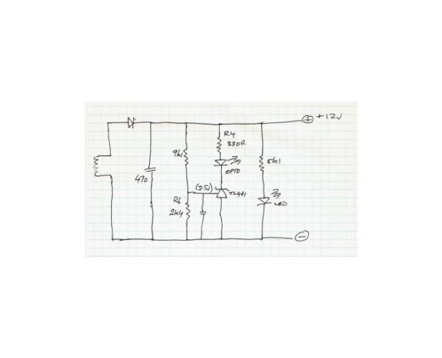
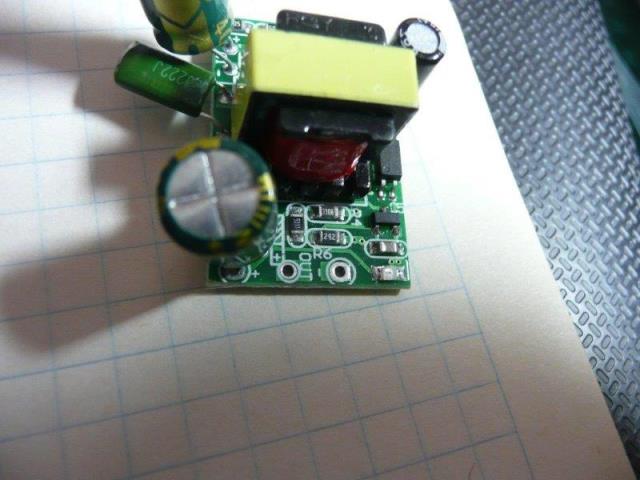
Isolated power supplies were always a bit expensive. I make my own but now there are some cheap ones becoming available. I do use these B1215S but dont ask too much of them. I have bought these XL-007 but I have not used them yet. We have good feedback on these units from Warp and Madness. These will take a DC input, perhaps as low as 35 volts. I have worked out the output circuit - see below. To adjust the output voltage: Easiest would be to change R6. ie, 1.8k (0603 smd) should give a 15v output. Cheers Andrew   |
||||
| Solar Mike Guru Joined: 08/02/2015 Location: New ZealandPosts: 1203 |
>> Isolated power supplies were always a bit expensive. I make my own but now there are some cheap ones becoming available. I do use these B1215S but dont ask too much of them. Yes I have made my own also, but they always end up being 3x the size of the commercial units, I now use the 2W versions of the above for multiple parallel mosfets. The XL-007 looks OK, thanks for drawing out the cct. Will order some and try them out. Cheers Mike |
||||
| LadyN Guru Joined: 26/01/2019 Location: United StatesPosts: 408 |
Andrew, thank you for the diagram. In the diagram above I see the first component which looks like a transformer winding. 1. Is that the secondary winding of the transformer from the board? 2. The primary winding was not drawn because it connects directly to the AC input? 3. If so, won't having any snubbers across the AC input and having it feed directly into the primary winding cause some EMI issues? |
||||
mackoffgrid Guru Joined: 13/03/2017 Location: AustraliaPosts: 460 |
Natasha, that is the secondary. No, the primary side is rectified then is using some sort of switch mode circuit to drive the primary. I just wasn't interested in it as I wanted to manipulate the output voltage. All you have to calculate (for your desired output voltage) the resister divider so that the voltage across R6 is 2.5v, the reference of TL431. The opto provides the feedback to the switcher. This ISO psu is about the best value going. No good in my current 24V project but great for 48V and above. Cheers Andrew |
||||
| Warpspeed Guru Joined: 09/08/2007 Location: AustraliaPosts: 4406 |
Those used to be available with 15 volt outputs, but I haven't seen those 15 volt versions advertised for many months. If you need 15v you can use a 12v supply and change R6 from 2K4 to 1K8. That will get you about 15.1v regulated output. It will no longer supply the full maximum specified rated output current, but as an isolated gate driver supply it will have plenty of surplus power. I run seventeen of them in my inverter. One provides +5v for the driver board, and there are four +15v supplies in each of my four bridge inverters. All seventeen running only consume slightly under 5 watts, which is the total running power for all the electronics in the whole inverter (with the four output transformers disconnected). Cheers, ĀTony. |
||||
| LadyN Guru Joined: 26/01/2019 Location: United StatesPosts: 408 |
Perhaps that is the reason why those 15 volt versions are not being offered anymore because people mostly order the 12V ones and those who need higher just modify it. As a result, the seller is not seeing a lot of demand for those 15 volt versions I had this question: why not run the two highside FETs from one rail from one single of these PSUs and the two lowside FETs from another rail from one single of these PSUs? In an HBridge only one pair of the FETs are drawing power at any time, right? would you happen to know (or guess?) the surge/peak demand from the FET's capacitance on these PSUs? |
||||
| Solar Mike Guru Joined: 08/02/2015 Location: New ZealandPosts: 1203 |
>> would you happen to know (or guess?) the surge/peak demand from the FET's capacitance on these PSUs? This is determined by the number, type of mosfets being used and their switching rate, look in the devices data sheet for the total gate charge in nC, then you can work it out: IRF4468 below. High-side mosfets will require 2 isolated supplies per bridge (hint source voltages are not the same) Cheers Mike |
||||
| LadyN Guru Joined: 26/01/2019 Location: United StatesPosts: 408 |
From: https://www.thebackshed.com/forum/forum_posts.asp?TID=11169&TPN=5 OK, so please let me know if I am wrong: 1. in theory, setting Vgs to GND should turn off the FET 2. In reality, it takes a while to drain Cgs, so to expedite the discharge process, engineers sometimes set Vgs to -0.7 (WHY? -0.7. Why not say -Vgs_max?) 3. At all times we must be mindful not to exceed +Vgs_max. To ensure this a zener rated Vgs_max might be useful but zeners are not as fast as TVS diodes, so if possible to source a TVS with Vgs_max, prefer that over a zener Did I get all of them right? |
||||
| Solar Mike Guru Joined: 08/02/2015 Location: New ZealandPosts: 1203 |
Specs for the higher powered mosfets for gate voltages are approx +-20v. some are 30v sensitive gate versions are +-10 approx. So the device doesn't careless if its gate is driven -ve with respect to source pin. I think what Poida was alluding to is some of the driver chips wont tolerate a negative common drive voltage beyond a limit and the tvs diode may help that, it will certainly protect against higher voltages, for -ve voltage I would use a shottkey diode in that situation to clamp -ve swings. Generally this is not an issue with correct gate drive design. Mike |
||||
| Warpspeed Guru Joined: 09/08/2007 Location: AustraliaPosts: 4406 |
These days just about all dedicated mosfet gate driver chips are CMOS digital devices with a high power CMOS output stage. Chips like the IR21xx series and TC4452 or the HCPL3120 opto isolated device for example. These all have complementary mosfet outputs and the mosfets have an internal source drain diode that protects the output mosfets from voltage transients caused by excessive ringing. So you don't need to take any special precautions beside fitting a suitable scaled gate resistor between driver output and each mosfet gate. Now there are quite a few switch mode control chips that can drive mosfets directly. These control chips often contain a LOT of internal analog circuitry and very often are built with bipolar transistor technology throughout. The power output stage will use an NPN and PNP pair of bipolar transistors. If these are hit with voltage spikes or excessive ringing, the lower NPN device particularly can latch up to the internal substrate if driven far enough below ground potential, which can be a disaster. With these biploar transistor types of chips, there are big warnings about this in the application notes, and external Shottky diodes are always recommended to protect from large negative transients. Always read the application notes for any chip you plan to use, and follow any advice exactly. The CMOS devices are pretty bullet proof, but bipolar transistor devices need special care and attention. Cheers, ĀTony. |
||||
| The Back Shed's forum code is written, and hosted, in Australia. | © JAQ Software 2026 |