
|

|
Forum Index : Electronics : Mikes Alternative Inverter
| Author | Message | ||||
| Solar Mike Guru Joined: 08/02/2015 Location: New ZealandPosts: 1203 |
Thought I would post this show progress on a new inverter build design based on a more modular architecture. I have a requirement to build a low power device of 2kw with a short term peak of approx 6kw and another of 5-6kw continuous with a peak of 15kw for 30 minutes or so. So two inverters, just different power requirements and high sustained peak power. Starting with the standard H Bridge design, have opted for a modular approach using isolated driver boards for each section. For mosfets have gone for IRFP4468 with 1-5 devices in parallel each driven by a high current totem pole driver. I like these totem pole drivers, they are cheap (50c), very small, can be mounted very close to the power devices and have independent control on source and sink drive currents. Each driver pcb is soldered direct to mosfet pins by a solder blob. The bigger inverter will use all 5 parallel mosfets in each leg and be water cooled. Driver: PCB: Will post some more photo's of the prototype as I get it built. Cheers Mike |
||||
| Warpspeed Guru Joined: 09/08/2007 Location: AustraliaPosts: 4406 |
Excellent design there Mike, very well thought out. Have to agree, modular approach with completely isolated grounds fed from continuous isolated dc power is definitely a giant step forwards. I am having great success right now with the following circuit which you might be interested in experimenting with yourself. to drive your quarter bridge. It has the following features: Cross conduction protection. Adds any amount of symmetrical dead time very simply. Very high noise immunity. Fully isolated grounds. Only one single twisted pair required to drive each half bridge. 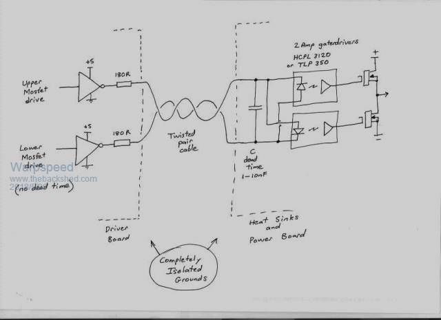 Cheers, ĀTony. |
||||
| yahoo2 Guru Joined: 05/04/2011 Location: AustraliaPosts: 1166 |
After a good 30 minutes staring at Mike's PCB I was pretty sure I had a handle on what is going on. now I am confused again, Tony, can you explain what you mean by fully isolated ground. or rather how it is considered isolated? my understanding of this is very poor. I am keen to build some DC motor drivers with a few of these little water cooled beauties, 1200volt 550 amp, they come out of 3 phase UPS systems for big server farms. they replace them after 12 months. it should be possible to make a board clip straight onto the pins. if I dont blow to many up I would like to have a crack at an inverter power board/block with these eventually. 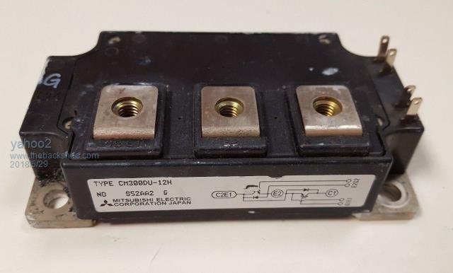 I'm confused, no wait... maybe I'm not... |
||||
| Tinker Guru Joined: 07/11/2007 Location: AustraliaPosts: 1904 |
Sorry Mike if this hijacks your thread but Tony's little circuit above has me intrigued. So Tony, If one feeds 180 degrees out of phase sine waves into the driver board on the left this would do the trick? And that little capacitor (1-10nF) adjusts the dead time? This is too simple, I think I'm misunderstanding something here? Is the other half of the bridge identical? Klaus |
||||
| Solar Mike Guru Joined: 08/02/2015 Location: New ZealandPosts: 1203 |
No problem, go for it, Tony's circuit and additional info is relevant to the topic. Mike |
||||
| Warpspeed Guru Joined: 09/08/2007 Location: AustraliaPosts: 4406 |
The whole suggested gate drive circuit is built around a pair if fairly fast gate driver opto isolators, but the sneaky part of it is the LEDs in the two opto isolators are connected head to tail. That way its IMPOSSIBLE for both opto isolators to turn on together. Its an effective last line of defense against cross conduction. Drive of one polarity turns on one LED, but positively turns the other one off. But to do that, the drive current must pass momentarily through zero to change polarity. Now most of these gate driver opto isolators are designed to have pretty equal time delays through the device when switching either on or off. So if you just do the inverse diode trick the circuit will work pretty much as expected and have very little or zero dead time. Now if we connect a capacitor in parallel with the inverse LEDs and we suddenly switch over the drive polarity, the slewing in voltage as it passes through zero can be slowed down. The capacitor must charge and discharge through the two LED current limiting resistors. It will spend some amount of time below both LED threshold voltages, where both LEDs are off, and create for us some dead time. (10nF gives about 2.5uS with the above circuit) Dead time is often created with an RC network and a diode for each gate driver. Six components for the drive to two mosfets. My circuit only requires one capacitor to do the same thing, and its symmetrical switching both ways. Extended gate driver wiring can easily introduce some extra problems due to induced noise, and the potential for false turn on. Any momentary false turn on usually creates the classic unexpected big bang blow up. Noise can be introduced through grounding problems between a lower mosfet source, and the ground at the driver circuit board, which might come from the battery. The IR2110 family of driver chips allow for this, but there are definite limits. The lower gate driver is not fully isolated as well as the upper gate driver. With very high power circuits, fast noise spikes of several volts can easily be generated between the two grounds, and that can easily be more than an IR2110 can handle. A much better approach is to treat the lower mosfet exactly the same as the upper mosfet and completely isolate the drive circuit from any common ground. Mike has done this with his four identical module approach, and its a highly recommended method for higher power applications. Another source of noise induced into long gate drive connections could be stray coupling to heatsinks that are actively switching, and nearby cables carrying high current at 23.4 Khz. Ribbon cables might be tempting fate a bit, but a lot depends on actual wiring and the physical layout. A twisted pair, with a capacitor across it at the far end, and actively driving the "off" opto isolator in the reverse direction all aid in increasing the immunity to noise introduced into very long gate driver wiring. Another thing many people never think about is what happens as all the various supply voltages initially slowly rise and slowly collapse as the main dc power to the inverter is switched on and off. Not all the different lower voltage dc supply rails will react together or in any particular sequence. If its possible for some brief transient condition to turn on upper and lower mosfets simultaneously, again we have the possible unexpected big bang situation. All this needs to be very carefully thought through, and multiple layers of protection provided, and it all becomes a lot more critical as the power level increases. Cheers, ĀTony. |
||||
| Tinker Guru Joined: 07/11/2007 Location: AustraliaPosts: 1904 |
Thanks for that explanation Tony. I did not spot your opto diode trick connection at your first sketch, very clever indeed. Klaus |
||||
| Warpspeed Guru Joined: 09/08/2007 Location: AustraliaPosts: 4406 |
This is my own much lower power version of Mike's modular approach. It essentially follows Mike's design philosophy of complete optical isolation, and with continuously running isolated dc to dc power sources. (no common grounding, and no voltage pump for the upper driver) The only significant difference is that mine only has to switch at 50Hz and drive a single upper and single lower mosfet. Mike's is for serious high frequency PWM, and vastly higher power, where the individual high current gate drivers become much more necessary. 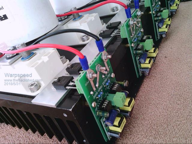 Cheers, ĀTony. |
||||
| Tinker Guru Joined: 07/11/2007 Location: AustraliaPosts: 1904 |
Tony, I can pick up lots of ideas just looking at your workmanship. I was wondering how you get the Mosfet legs far enough off the heatsink so they are not too close with using the Dinkle terminals. Now I see, mount the Mosfets on a Alu flat bar - simple, effective  . .Is there anything interesting inside those white 'bases' your capacitor busbar mounts on? Another question, which isolated DC/DC converter are you using? I was looking at this one:DC/DC Klaus |
||||
| Warpspeed Guru Joined: 09/08/2007 Location: AustraliaPosts: 4406 |
Klaus, I am using these: https://www.ebay.com.au/itm/New-AC-DC-Power-Supply-Buck-Converter-Step-Down-Module-5V-12V-3-3V-9V-24V-500mA/262807265342 ?ssPageName=STRK%3AMEBIDX%3AIT&var=561802963756&_trksid=p2060353.m1438.l2649 Available in a variety of output voltages, but at the moment 15v ones seem to have become extinct. These start up at around 60v input, not much good for a 48v system but o/k for my 100v system. I now have eight, but need eight more for the two much larger bridge inverters on the other side of the same heatsink. Those big white things are 1200v 200 amp half bridge IGBTs. Just like the picture of the big black 350 amp one Yahoo2 posted earlier. I plan to use the same identical driver boards for those, as for the smaller individual mosfets. These will have 5mm pitch plugs and sockets instead of screw terminal blocks. This picture gives a better perspective of the mosfet pins and screw terminal blocks. Still short of many parts which should hopefully arrive over the next few weeks. 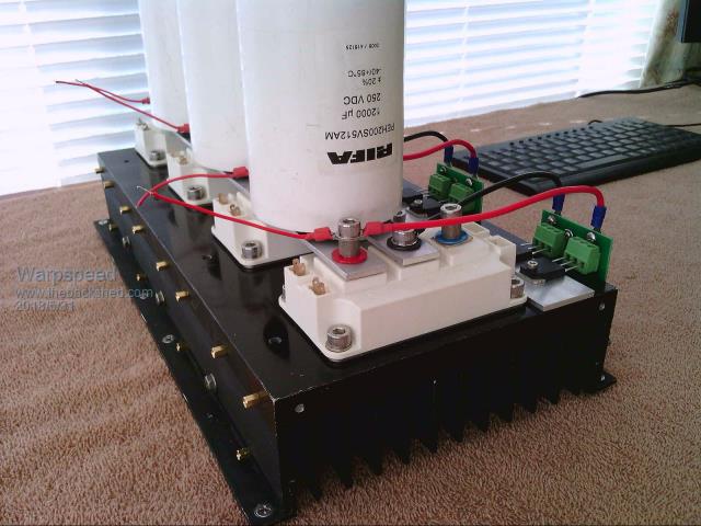 Cheers, ĀTony. |
||||
| Tinker Guru Joined: 07/11/2007 Location: AustraliaPosts: 1904 |
But these are AC/DC converters. The inverter has to be up running before AC is available. And to get it running I will need 12V DC from the battery. Is there something I'm not getting? Klaus |
||||
| Warpspeed Guru Joined: 09/08/2007 Location: AustraliaPosts: 4406 |
The input to these modules is a bridge rectifier and 470uF cap. They work fine on any dc voltage from about 60v up to 400v, and they are not a buck regulator but a fully mains isolated flyback converter. Cheers, ĀTony. |
||||
| Solar Mike Guru Joined: 08/02/2015 Location: New ZealandPosts: 1203 |
Gosh Tony that is a really clean professional build, impressive. Good input on the opto driver, I may use that. Have made some more progress on my prototype, as I want a modular system will build this prototype on a sheet of 5mm aluminum, this will act as heat-sink and be one side of the main enclosure, extra cooling fins can be bolted externally as required. Mosfets are mounted on 16mm x 50mm alloy flat bar bolted to the base via a silpad for insulation with 5mm nylon countersunk screws. The bars carry power and with a good surface area for heat transfer to the base plate. Copper bar 90mm^2 joins the +ve connections, center is 0v, two others are transformer connections. Copper to alloy jointing compound is smeared on all connections prior to cleaning off oxides and clamping up. 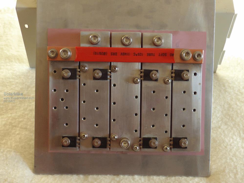 Mosfets are bolted to the bars with 4mm screws, source legs are clamped between two copper washers, other pins are chopped short and bent up on the ends for connections to the driver boards sitting across each row of devices, blob of solder makes each connection. I discovered the base of these mosfets are not very flat, they sit on high spots 2-3 thou which isn't good for power or heat transfer, quick lapping on a flat surface on a sheet of 600 wet and dry emery paper and kero fixes that, some are worse than others, final thin smear of cable jointing compound prevents oxidation on aluminum and exposed copper surface of mosfets. 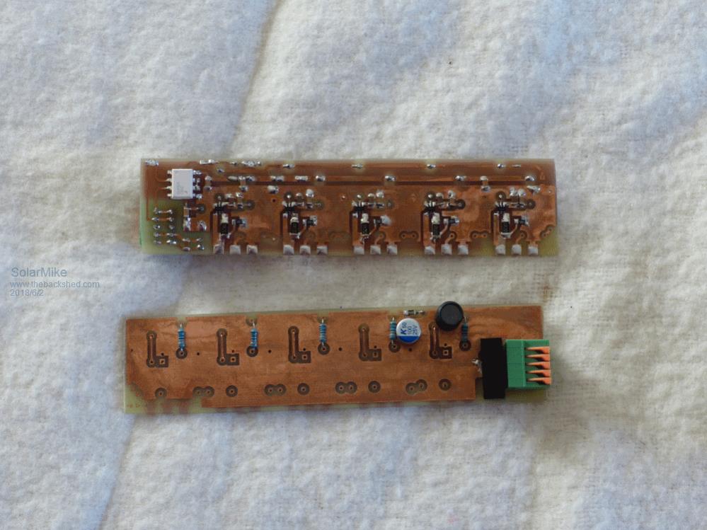 Decided to mount the capacitors on a pcb that sits above the mosfets, there are myriads of options here depending on what caps you have, big low esr types are very expensive, so have used many smaller ones in parallel, this has the advantage of good pulse current and thermal cooling, their esr's are all in parallel and coupled with a 1uf smd ceramic across each device gives a very low impedance capacitor bank; shown are 24 x 3300uf. 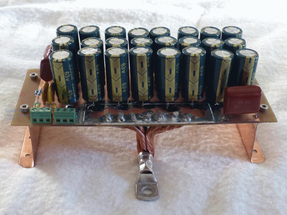 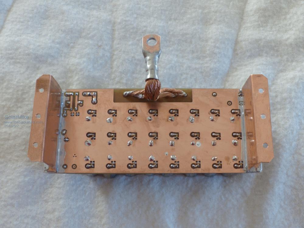 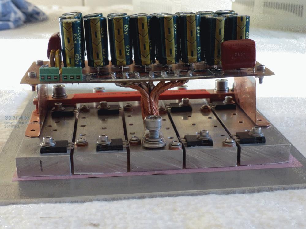 Now I need to make a spwm drive to test it, again lots of options, I like where Mad is going and others with Arduino's for control and drive signals, however I am with Oztules here a bit and perhaps prefer a simpler solution, so armed with an XR2206 sine generator chip , a PCM generator chip along with a few op amps, will see what I can come up with. I see no reason to not employ a simple analogue chip based solution for the bipolar spwm driver, and use a higher pwm frequency of 50 khz or more so smaller transformer chokes can be used. Cheers Mike |
||||
| Warpspeed Guru Joined: 09/08/2007 Location: AustraliaPosts: 4406 |
Now that is a superb example of optimum high frequency layout and thermal design. A real inspiration, and very original too. The analog derived PWM should definitely work, the class D audio guys have been doing something very similar for a long time. Cheers, ĀTony. |
||||
| The Back Shed's forum code is written, and hosted, in Australia. | © JAQ Software 2026 |