| Author |
Message |
Solar Mike
Guru

Joined: 08/02/2015
Location: New ZealandPosts: 1203 |
| Posted: 04:01am 27 Jul 2022 |
 Copy link to clipboard Copy link to clipboard |
 Print this post |
|
I looked at a multiple phase PV charge controller a year or so ago, the prototype used an RC delay line to obtain the various delays for each phase; unfortunately it didn't work that well as the granularity of the delay timing was too large, not allowing full range of PWM duty cycles.
I am revisiting this in order to use smaller power components - inductors, mosfets and Schottky devices in each phase, then combine their outputs to the battery. The common high voltage (250V) Schottky diodes only have a 40 amp current rating, combining multiples of these in parallel to get a higher current is very bad design and doomed to failure; - note this doesnt apply to Silicon Carbide devices with their positive temperature coefficient. Its also easier to make small 30 amp inductors than 60 amp monsters and a lot cheaper.
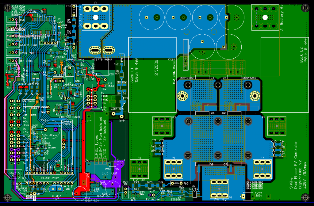
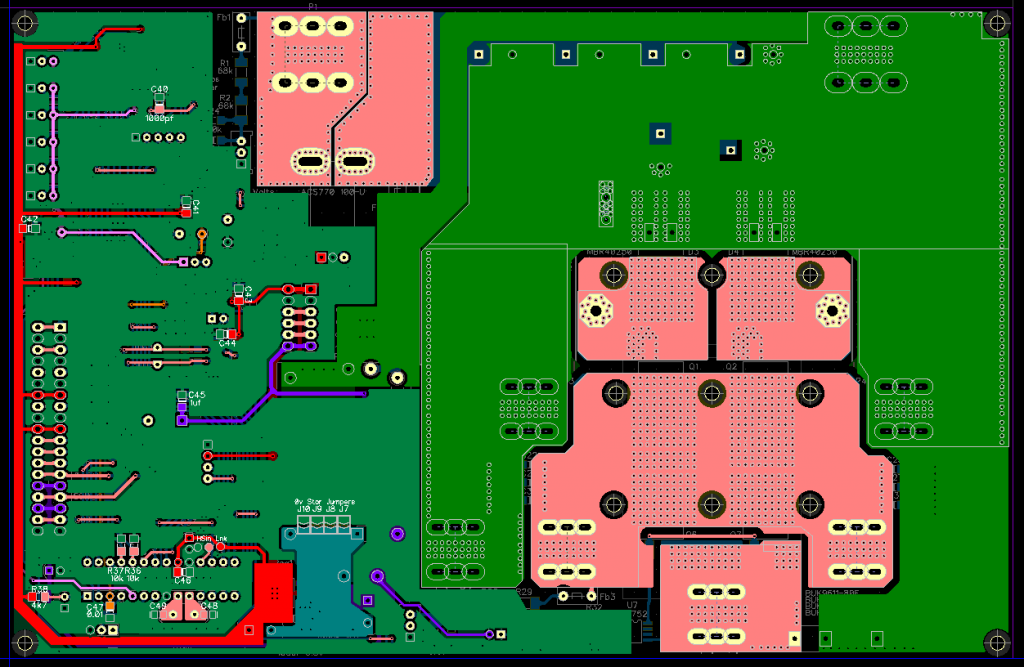
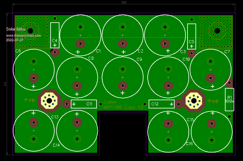
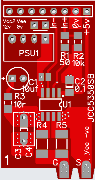
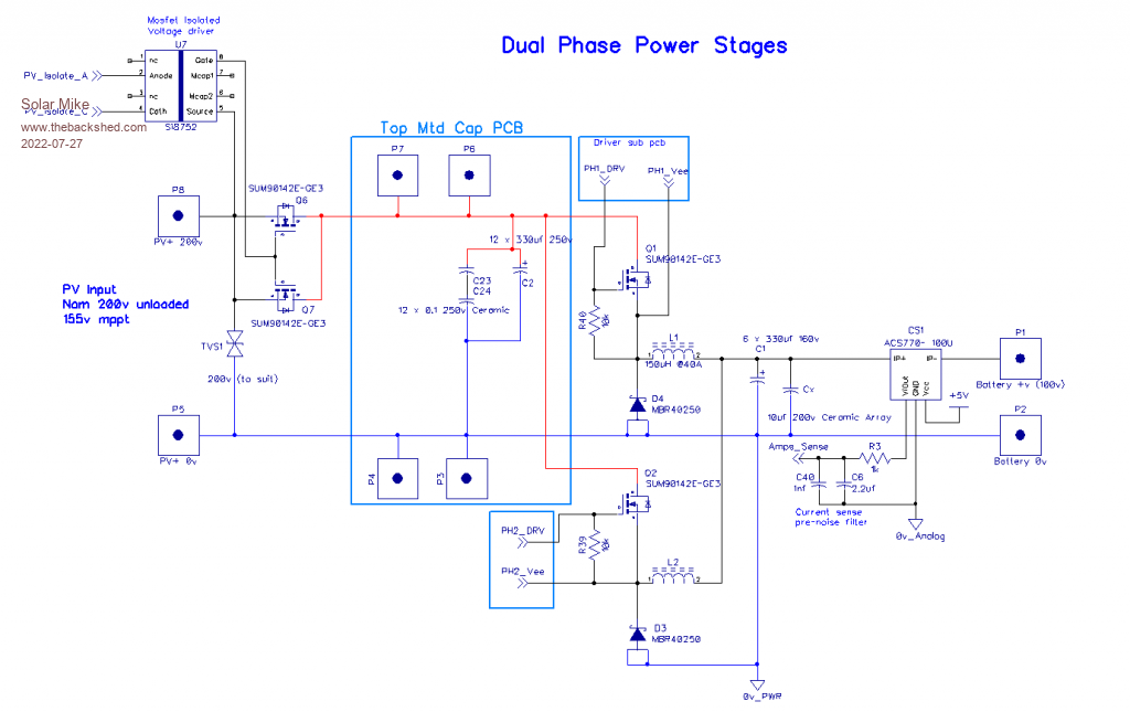
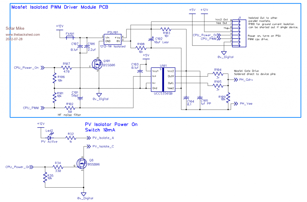
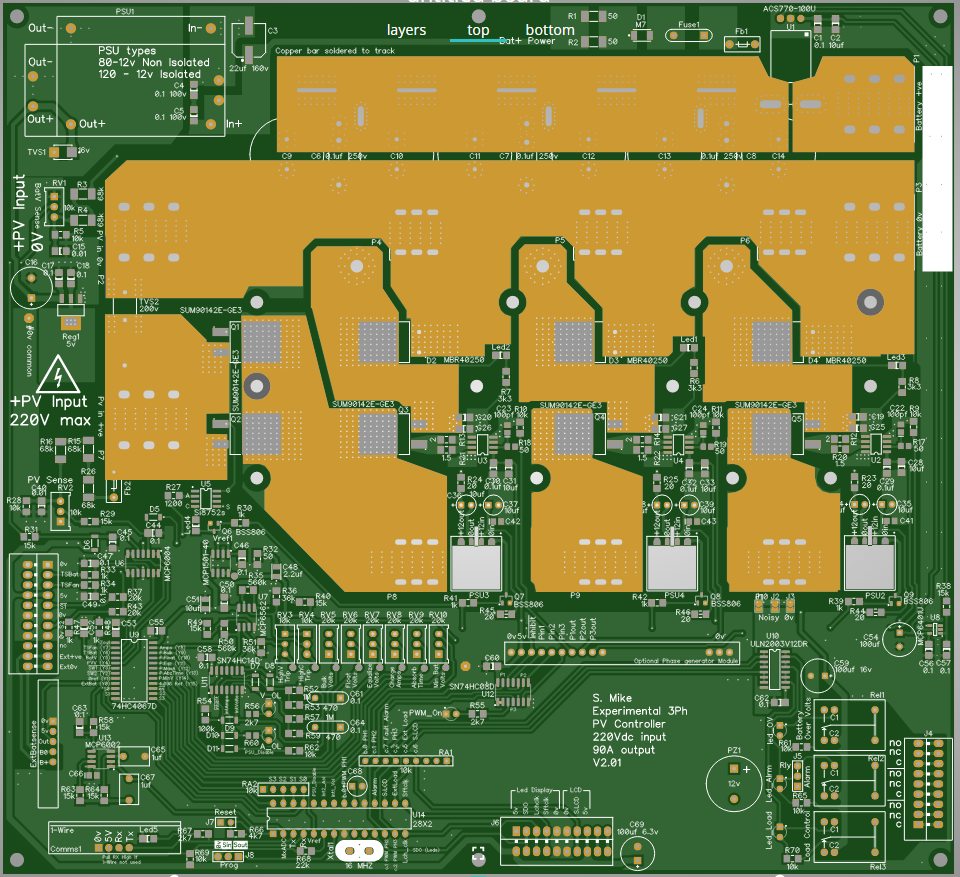
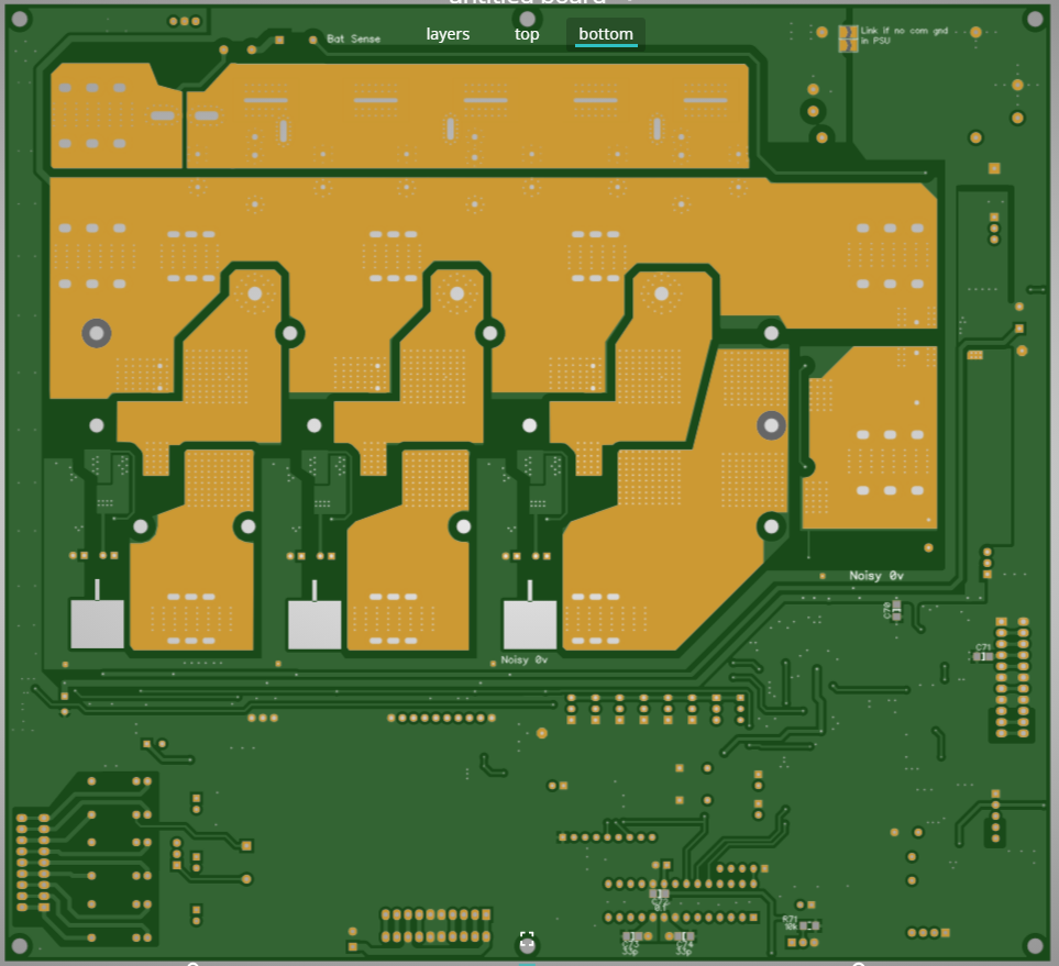
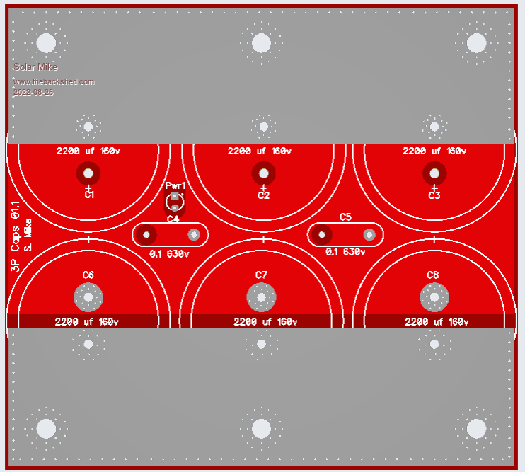
This non-synchronous design has two phases or buck converters, with a common PV supply capacitor bank and final output caps. Each buck inductor mounts on the main PCB, the mosfets and schottky devices solder to the top side, conducting their heat through the vias to the bottom that sits on a silpad then alloy plate on the heatsink. The main PV electro's sit on a separate pcb Hat above, connected via P3,4,6,7. The buck mosfets have little driver pcb's soldered vertically off their pins. Not sure what the max current output will be, looking forward to testing to destruction.
Now that the initial design has been laid out, will draw enough of the schematic to double check in case I have misplaced a connection or two, main pcb is 225 x 146mm.
Top:
Bottom:
Caps:
Driver:
Cheers
Mike |
| |
Solar Mike
Guru

Joined: 08/02/2015
Location: New ZealandPosts: 1203 |
| Posted: 11:54am 27 Jul 2022 |
 Copy link to clipboard Copy link to clipboard |
 Print this post |
|
Schematic part for main power stage (buck).
Mike |
| |
Solar Mike
Guru

Joined: 08/02/2015
Location: New ZealandPosts: 1203 |
| Posted: 01:06am 28 Jul 2022 |
 Copy link to clipboard Copy link to clipboard |
 Print this post |
|
Schematic part for mosfet drivers.
So far no changes to pcb.
Mike |
| |
Solar Mike
Guru

Joined: 08/02/2015
Location: New ZealandPosts: 1203 |
| Posted: 12:55am 30 Jul 2022 |
 Copy link to clipboard Copy link to clipboard |
 Print this post |
|
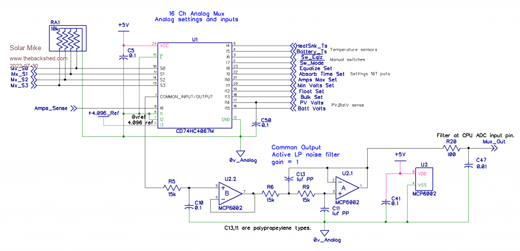
Schema for the 16 ch analog mux:
In the past I have used multiple CPU ADC input pins and an accompanying active noise filter, to simplify things its easier to use a mux chip followed by a single 3rd order active low pass filter.
MPPT control measures the PV volts and charge current every 200 mSec, this gives plenty of time for the input to be selected and stabilize. The various charge settings inputs are �20K 10T pots with a precision reference source, 4.096V; this is also applied to the CPU ADC +Ref pin.
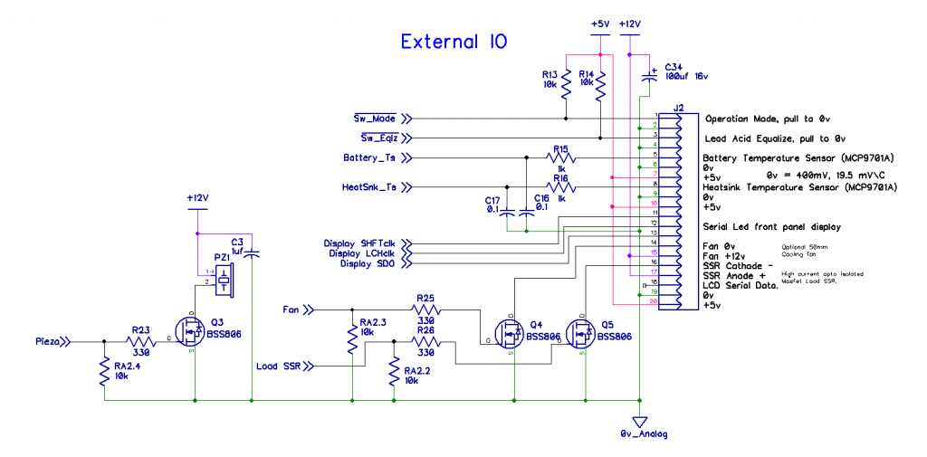
Schema for the external IO:
A 20 pin spring loaded connector used here, connections to the active temperature thermistors (MCP9701), various manual switches, LCD serial display, 50mm fan and external high power SSR load switch.
Note I don't use the DS18B20 temperature sensors as the CPU clock changes frequency to talk to them, stuffing up the PWM drive.
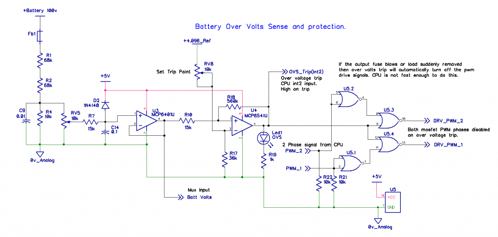
Schema for Battery Volts Sense:
Battery sample taken off RV5 via op amp buffer, same sample is also used for fast over voltage protection using comparator U4; if the charger is under high load and is suddenly removed, the output voltage can rise faster than the CPU ability to control by reducing PWM duty. The comparator trip point is set to about 10V higher than normal and will disable the PWM drive signals, allowing the CPU to catch up; this would not happen if the code was written in assembly or C+, basic is a little slow. I really must learn PIC assembler, used to spend 1000's hours writing Z80 assembler many years ago.
So far there have been no errors on the pcb, however I have re-run several traces and split the 0v common into 3 zones rather than 2 for better noise control. I won't bother doing any more circuitry, will fire off the gerbers and some point in the future publish the results back here.
Cheers
Mike
Edited 2022-07-30 10:58 by Solar Mike |
| |
Solar Mike
Guru

Joined: 08/02/2015
Location: New ZealandPosts: 1203 |
| Posted: 12:09pm 26 Aug 2022 |
 Copy link to clipboard Copy link to clipboard |
 Print this post |
|
While waiting for the boards to be made have concocted a 3 phase version using the larger 28X2 cpu. It has more pwm channel timers so can be tweaked to produce 3 phase outputs, in theory anyway and from software tests on a bread board.
I don't know whether the 3 phases will stay in sync, if it doesn't work out have allowed for a plug in module with a RC delay line using 6 x 74HC14 chips (36 small delays) to create the required output.
The common shared input capacitor bank sits on a hat pcb above the main board, have made a couple to suit differing electro sizes.
Copper bus bars run under the capacitor module and also soldered to the output tracks. If I limit each phase to nominal 30 amps then combined will be 90 amps.
I was going to use this design to run off an isolated 2KW DC supply to charge the battery bank from a generator.
Cheers
Mike |
| |

